Quantcast
Channel: Sustainable Suburbia
Viewing all 234 articles
Browse latest View live

Digital Dust - A further Journey into Nano Computing?

$
0
0
This week I have been working on various MSP430 projects including a prototype board based on the MSP430FR2433.

This is a very small chip in a 4mm square package - which doesn't make it really easy to work with - so I decided to design a series of small boards to take full advantage of its diminutive package size.

Today I have been laying out possibly what is the smallest board I have done so far - just 10.24mm x 12.7mm.  Remarkably this includes the breakout for the MSP430FR2433 plus an external SPI memory device.

Nanode 2016  - Just 0.4 x 0.5" 
As you can see, things are fairly compact on this board, and I have had to use 0402 resistors and capacitors -the layout was  surprisingly  easy for a board of this density. All of the components are on the top side - except for an optional additional memory device and an extra decoupling capacitor.

Despite it's small footprint, this is a full microcomputer with up to 256K bytes of external memory.  It has 3 communications interfaces which can include up to 2 UARTS and up to 3 SPI ports.

If you are using it with a serial terminal, with one UART dedicated to that purpose,  there are a further 14 GPIO lines available - 6 of which have a 10 bit ADC function.

The board is designed to take external memory - which may be either SRAM or FRAM, or a mix of each. If FRAM is used, then the device will retain the contents even after power down.

This module has been designed as a building block, primarily to be used to interface with SPI based peripheral devices - or where space is too tight for even an Arduino Nano.


Building WiNode 5 - Part 4

$
0
0
WiNode Lives!

After a weekend of hard graft, I have some samples of the WiNode 5 board in various states of build - with three of them up and running code.

I also built up one of my FT812 "EVITA" video boards so that I could try it out with WiNode:

All in a Weekend's Work when the day job doesn't get in the way!
WiNode - The Core of  a Neo-Retro Computer Project!


Since it's beginnings in early December, the project for this year is a Neo-Retro computing platform. It was just a case of identifying the right hardware and getting on and making the pcbs.

The platform has it's heritage in Arduino - hence originally the use of an ATmega1284 microcontroller, the Arduino style headers and the stackable shields.  

However a new MSP430 FRAM based microcontroller core that plugs right into the central 40 pin DIL socket is under construction - and is likely to become the preferred processor.

The fact is that we have a complete 8-bit computer with high-res colour graphics, PS/2 keyboard and mouse shoe horned into something about the size of a fag-packet. The bulkiest part of this design is the VGA connector and cable!

This is most definitely not a Raspberry Pi, nor any thing similar.  It is a working 8-bit (or 16 bit) computing platform made from about £20 ($30) of components.

 "Hello world" WiNode 5 and EVITA stacked together
It does not run Linux, nor does it need megabytes of someone else's firmware to make it run. It's just a simple platform with which to experiment

Brief Summary:


On the EVITA GPU shield

PS/2 Keyboard
PS/2 Mouse
FT812  (Gameduino 2)

On WiNode 5

RFM69 Wireless Module
FM25W256-G  32K x 8bit SPI FRAM
micro SD card
ESP-01 WiFi


Experimenting with New Devices - Part 3

$
0
0
In this short series of posts, I have looked at alternative processors to the ATmega1284 for my "Neo-Retro" Computing platform - based on my WiNode 5 and EVITA board stack.

WiNode 5 - shown below, has a 40 pin DIL socket located in the centre of the pcb. The position of the signal pins on this socket are arranged so as to accommodate a Atmel ATmega1284 - as this is a commonly available, reasonably low cost AVR device with 128Kbytes of Flash and 16Kbytes of RAM. It also has the added advantage of two uarts, SPI, I2C and 3 interrupt lines - making it kind of a "super-Arduino".

WiiNode 5 with ATmega1284 40 pin DIL version fitted
However the socket was not solely intended for the ATmega1284.  It is for generic access to the hardware on the WiNode board - and so any microcontroller, fitted to a suitable 40 pin carrier board, may be fitted in this position.

Recently, in this Blog, I explained how the 40 pin DIL package was a neat way of packaging up some of the smaller microcontrollers, so a s to make them more manageable in the form of a plug in module - that does not require difficult SMT soldering.  This time I take a closer look at the 40 pin format - and show how it can be used to our benefit, for a number of different applications.

As a teenager, growing up in the very early 1980s, the 40 pin DIL was the only format that microprocessors came in.  It was a convenient size that could carry a 16 bit address bus, an 8 bit data bus, a few control lines and power. Some manufacturers even copied the pin-out of their competitors' devices - so that they could swap their devices for their superior device - although this practice usually ended in law suits.  However, it's not a bad idea to have a common footprint amongst devices - making the upgrade path very simple.

So with this in mind I have decided to do something similar, and make a series of compatible modules that allow the user to move conveniently between processor families.

A Common Template for a Microcontroller Plug-In

Making a plug-in module is a fairly trivial process - it's just a  small piece of pcb with a standard pinout, which acts as a chip carrier for whatever devices are needed in the design. I did this a couple of years ago with my STM32F373 based ARMiGo project.

First we look at the template for the proposed module.  You will recall that the ATmega1284 is available as a DIL 40 package - and its arrangement of ports allows form a very logical layout with power pins at the centre - which prevents disasters, should you happen to get the IC into the socket the wrong way around! So by the miracles of ASCII-Art in plain courier font we have the package template.

                    ATmega1284 Package
                    ________________
                B0 |o 1            o| A0   A   I
                B1 |o              o| A1   n   n
          INT2  B2 |o              o| A2   a   p
          PWM0A B3 |o              o| A3   l   u
          PWM0B B4 |o              o| A4   o   t
          MOSI  B5 |o              o| A5   g   s
          MISO  B6 |o              o| A6   u
          SCK   B7 |o              o| A7   e
            /RESET |o              o| AREF
              VCC  |o              o| GND
              GND  |o              o| AVCC
             XTAL2 |o              o| C7 
             XTAL1 |o              o| C6
           RXD1 D0 |o              o| C5
           TXD1 D1 |o              o| C4
           RXD2 D2 |o              o| C3
           TXD2 D3 |o              o| C2
          PWM1A D4 |o              o| C1  SDA
          PWM1B D5 |o              o| C0  SCL
          PWM2A D6 |o              o| D7  PWM2B
   
Note that the power pins are in the centre of the package and offset - so cannot be reversed accidentally. Additionally the ports A,B,C,D are neatly stowed in a way that makes navigating around the pinout very easy - it's all done for maximum simplicity.

I have also labelled the key signals - so when it comes to layout the new processor module - it's a case of matching up function on a pin by pin basis.

  
With  the template for the package in place, it is now possible to lay-out any small processor in this format.

My interest lies in two (or possibly three) candidates.   Firstly the 38 pin TSSOP MSP430FR5759 secondly the 48 pin LQFP STM32Fxxx ARM M4 Cortex device. Both of these will be capable of a significant improvement in processing throughput over the original ATmega1284.

An MSP430 FRAM Variant for WiNode 5

Last week, whilst waiting for some pcbs to come back from manufacture I had a quick look at the MSP430 range of microcontrollers - especially those in the MSP430FR5xxx series which have non-volatile ferroelectric memory.

This time I look at some of the more practical aspects of using these interesting SMT devices.

These are available in a relatively easy to use 38 pin TSSOP package, so the plan was to make a neat little TSSOP to 40 pin DIL adaptor board - so that they may be used with breadboards and stripboards.

After a little thought, and a few hour's with EagleCAD, I came up with the following layout.  The device is uncluttered - for once, I am not trying to squeeze every last component onto a small board.

The board carries the MCU, and external SPI memory device, a 32kHz crystal,  Reset Button, User Button and a LED. In addition there is an external SPI memory device  - which can be FRAM (up to 256Kbytes) or SRAM (up to 128Kbytes).

A simple 40 Pin DIL Breakout Module for the MSP430FR5739 and MSP430FR59xx devices


Bootloading Blues

$
0
0
A previously unpublished posting from February 9th that has launched me on a wonderful voyage of discovery of the MSP430 series of microcontrollers.

As Kennedy said in September 1962...

We choose to go to the Moon! 

We choose to go to the Moon in this decade and do the other things, not because they are easy, but because they are hard; because that goal will serve to organize and measure the best of our energies and skills, because that challenge is one that we are willing to accept, one we are unwilling to postpone, and one we intend to win ...

But first we need a working Rocket!

We have an on-going project at work, which needs an MSP430 bootloading over it's serial port with a hex file.  So we went out and bought the cheap open source, Rocket BSL programmer from Olimex.

I then found that I needed the drivers and other software from TI,  which I had to register for and then declare to the US Government that I wasn't going to use it against America in any way, shape or form.  So far, so good.

North Korean? No, just Bulgarian.
The MSP430-BSL is described as a joint project between Olimex and Texas Instruments. The reality is that no-one really wants to take ownership of it, and there is no one specific site that you can go to that gives you everything you need to get this programmer to work.  It's like the code has been fragmented and spread to the four corners of the known cyber world - lest anyone dares try put the fragments together again and unleash the awesomeness of this great force on mankind. What I'm trying to say is that both Olimex and the Mighty TI have shot themselves in both feet, and it's no surprise that the MSP430  is languishing in some stagnant microcontroller cul-de-sac.

After mulling this over for a while, I began to think that proprietary bootloaders really suck.  There should be a universal tool which allows you to squirt code from a hex file into any microcontroller, from any platform.  And that got me thinking about the humble USB-serial programming cable - such as those by FTDI, SiLabs or our Chinese friends who make the CH340.

It also appears that others have had this thought.  In my search for an alternative MSP430 programmer, I found this interesting approach from Flying Camp Design - a programmer that is literally not much more complicated than an FTDI cable - just an FT232R on a small pcb.

Bootloaders are usually designed to be small, and not particularly human-friendly, because they are normally talking to some proprietary application running on the pc.  But this doesn't need to be the case, there is sufficient flash space in the boot block of most micros to put a more sophisticated bootloader program - one which is actually capable of running some interpreted commands and presenting a more human friendly face to the user.


The March of MSP430 Progress

$
0
0
Mad as a March Hardware Engineer

We are almost 3 weeks into March, and already it has been a very busy month in terms of both hardware and software developments.

To give some context to my recent posts, I have recently taken on a new assignment at work, which is the creation of a new family of hand held instruments.  Some of the existing products use the MSP430 microcontroller, whilst another uses two Atmel AVR microcontrollers.

I wanted to eliminate the AVR from the mix - as the product has become too expensive to support, and at the same time rationalise the number of Vendors from whom we buy microcontrollers.

In relative benchmark tests, the 16 bit MSP430 is capable of about 2 to 3 times the processing throughput of the AVR,  but about half the thoughput of the ARM Cortex M0/M0+. On average the codesize for the MSP430 is about 70% of that used by the AVR.

Whilst I could have used ARM devices for the application, I already have the existing instrument code, and I suspect that it is easier to enhance the current code of the existing target, than port it to a new processor family.

However, what sealed the deal for me was that some devices in the MSP430 series have multiple 24bit Sigma Delta ADCs (intended for 3 phase electricity metering applications), plus there are parts with low power, non-volatile ferro-electric memory (FRAM) and segment style display drivers.

In the 10 years or so since the current instrument was designed, the active mode power consumption for the MSP430 has better than halved from about 280uA/MHz to 126uA/MHz. This will all help to prolong battery life, and possible reduce the number of batteries required.

Having decided to use the MSP430, I needed a crash course in how to use it - so about a month ago, I bought a few of the newer LaunchPad dev boards one featuring the MSP430FR4133 device with 6 digit segment-LCD, another with the MSP430FR5739 and a third with the MSP430FR5969 - which allows the active current consumption to be monitored. My two blogposts of February 17th describe these boards. I was also spurred on when I found that Jean-Michel Thoorens had written a "Fast Forth"for the MSP430FR5969. This I had to try.

In order to get started with the MSP430 series I downloaded the Code Composer Studio tools and tried a few example programs to familiarise myself with the peripherals. After getting the Blinky LED to flash, the next stage was UART send and receive to a terminal followed by ADC readings.


In order to set up with the  MSP430, I had to get the uart BootStrapLoader (BSL) to work. This was the first challenge , in moving to the new processor.   My blogpost of 26th February describes some of the difficulties I had.

With the BSL fully working I then started to look seriously at the MSP430 using the G2 Launchpad I was given free at the San Mateo Maker Faire in May of 2012.

My first task was to retrace my steps from a couple of years ago when I got my first MSP430 Launchpad and  tried porting my SIMPL tiny interpreted language to it using Energia - an Arduino-like IDE - but for the MSP430.  The exercise was a success, but as the MSP430G2553 only had 256 bytes of RAM, I was not going to be able to write a lot of code before the RAM was full.  In the blogpost of March 3rd - I look at the G2 Launchpad and both the MSP430GR2533 device and the MSP430F2013 device which has the advantage of a 16 bit SD ADC.

I studied the '2013's 16 bit SD ADC - as this was possibly going to be required in the final build. I also found some very useful helper functions for the '2013 called  "MSPEZIO" written by the University of East Carolina's Physics Department. I also explored the Universal Serial Interface (USI)on the '2013 - which is great if you want to send serial ay 16MHz!  My blog entry of March 4th looks at these topics.

However it was the shortage of RAM, again on the '2013 device that encouraged me to look for alternatives.  About that time I came across Rick Kimball's code for using the 23K256 SPI SRAM device on the USI.  I got his USI code running with a 23K256 and then modified the code so that it would work on the more modern Universal Serial Communications Inteface or UCSI - of which most Modern MSP430 devices have two or three.  My blogpost of March 5th describes these developments.

So one week after getting through the Bootloading Blues, I had serial comms, SPI and external SPI memory working. It was time to set about the challenge of putting this all together as an application.

For this I dusted down my SIMPL language and spent a Sunday afternoon and evening writing some code. The extended SIMPL was then christened SIMPLEX, and features in the two part blogposts from March 6th. It hard to believe that that was only 2 weeks ago. I now had a virtual machine running on the MSP430G2553 Launchpad which could execute code out of external SPI RAM - plus a bunch of other useful functions including a hex-dump facility.

Around about this time, my MSP430FR4133 Launchpads arrived - so I spent an afternoon porting SIMPLEX from the '2553 across to the more spacious '4133. This is covered in my blogpost of March 9th.


In Summary this post has covered the following  posts from between February 9th and March 9th


Bootloading Blues
The Great MSP430 Bootloader Swindle
More MSP430 Machinations
MSP430 Serial Communications
Interfacing SPI RAM and FRAM to the MSP430
SIMPL Meet SIMPLEX - Part 1 Putting it all together
SIMPL Meet SIMPLEX - Part 2 Running SIMPL code out of External RAM
Porting SIMPL Code to the MSP430FR4133 LaunchPad

The next summary post will feature the remainder of the Mad March MSP430 machinations, including some new hardware developments.


Beware the Ides of March

$
0
0
This is the second summary post for my weekly MSP430 activities.

I am at that age where if I don't write something down, I will forget it... and if I do write something down, I will forget it in about 2 weeks.......

In this post we cover the various hardware developments that have been made over the last few days.

ChipStick - a diminutive dev-board  March 13th

The "$5 Forth Computer" March 15th

Building a $5 Forth Computer  - First Steps   March 18th

Digital Dust - A Further Venture into Nano-Computing March 19th

Experimenting with New Devices - Part 3 "The FramStick" March 20th

ChipStick - An Small Scale Experimental Forth Machine

$
0
0
Last week, I wrote about the $5 Forth Computer, and showed an early breadboard version using an MSP430FR2433 mounted on a prototyping adaptor and plugged into a breadboard.

Well, I am pleased to report that the batch of 20 prototype pcbs have arrived back from the manufacturer earlier today and the build of the first unit is underway.

The following pictures show the build sequence - starting from the bare pcb


Top side of unpopulated ChipStick board - millimetre scale!
Underside of ChipStick pcb with locations for SRAM and USB converter IC


ChipStick with USB connector, regulator and MCU added


The ChipStick design has the following features:

  1. MSP430FR2433 with 15.5K FRAM and 4K SRAM
  2. External SRAM or FRAM device connected via SPI on USCI B0
  3. CH340G USB to serial converter IC on detachable section of board
  4. 3V3 voltage regulator
  5. Reset Switch and User LED
  6. 20 Pin DIL footprint to allow insertion into G2 Launchpad socket.
  7. Programmable by SBW or BSL

ChipStick - code loaded and Flashing LED (before sunrise)


Next Time:

Fast Forth - by Jean-Michel Thoorens

This is an implementation of a Direct Threaded Code Forth, written in MSP430 assembly language.  It communicates with a terminal program TeraTerm, at 921600 baud.

I have it running on an MSP430FR5739 - can I port it to the '2433 on te ChipStick?

ChipStick - Applications

$
0
0
Introduction

ChipStick is a tiny 16 bit microcomputer attached to a PC via a USB cable. It comes with up to 256K bytes of non-volatile memory - uniquely using ferro-electric memory.

It has up to 16 accessible GPIO lines - which include a mix of SPI, I2C, UART, Timer and ADC channels.

ChipStick may be plugged into a breadboard or stripboard and act as an intelligent programmable controller interfacing with other circuitry.

ChipStick can also act as a Digital Debug Tool (DDT), with jumper wire attached, - used to debug/develop low voltage (3V3) target hardware.

In each case, the extendable Scripting Language SIMPLEX may be tailored to the exact requirements of the user' application.

ChipStick is based on non-volatile ferroelectric technology.  This means that your applications and any recorded data remain in memory even after power down.

ChipStick may be extended in hardware to meet the requirements of the application - this is planned through both a series of larger expansion boards (based on low cost 50x50mm format) and stackable micro-modules that match the DIL 20 socket format.

Applications

With these primary applications in mind, ChipStick has been designed to be as versatile as possible - within the constraints of the small footprint.

As a debug tool, it is no bigger than a USB Stick - easily carrier around with essential hacking tools.

I have designed it as a socketable component that can easily be added to a board - where a small amount of intelligence is required, or for bridging between sensor devices. It can also collect or send data to SPI devices and bridge that back to the PC via the UART channel.

Equally, it could be used as a small test equipment device to exercise, monitor or control prototype hardware - it has 16 GPIO lines - including two full SPI ports. These can be attached to the target hardware, and using the SIMPLEX scripting language, the various target hardware can be exercised and data reported back to the PC.

With the right SIMPLEX script, it can be used to transfer a hex, bin or ascii file from the PC to the target under development.

The external memory may be used for sensing and datalogging applications, capturing waveforms, playing back arbitrary waveforms - as a signal generator.  The ADC channels may be used as a low bandwidth oscilloscope, test meter or for monitoring changing physical quantities in science experiments.

ChipStick takes much advantage from the trend in modern sensors and peripherals to connect via the SPI or I2C bus. The MSP430FR2433 device provides up to 3 separate SPI buses.

ChipStick can be interfaced to Wirelss and WiFi modules such as the RFM69 and the low cost ESP-01.

Suitable sensors include accelerometers, gyroscopes, digital compass, temperature, pressure, loadcells etc.

For basic GPIO operations - common shift registers may be used with the SPI bus such as the 74HC595 for 8-bits output - for driving LED arrays, the high power TPIC6B595 for driving stepper motors, and the 74HC165 for 8-bit inputs.

Using a LED driver IC - such as the MAX7219 or AS1100 series - up to 8 digits or an 8x8 array of LEDs may be driven from the SPI port.

OLED and LCD graphics displays may also be driven from SPI  with a couple of control signals.


Educational Applications

ChipStick as been designed with education and experimentation in mind.

It can be used specifically to assist in the teaching of electronics, computer science and interactive coding.

It is versatile enough to meet the needs of high-school and university undergraduates, plus simple enough meet the requirements of the maker and hacker community.

The small size of ChipStick allows it to be used to give intelligence and connectivity in situations where other technology is just too bulky to fit - with the programmer section detached it is only 26.5 x 11mm - small enough to fit inside a 4x2 Lego block!

It's low cost means that it can deployed in areas where other solutions might prove too expensive.

Here are a few of the educational applications:

Teaching Forth.


Forth is an interactive language and can be best taught with hardware that creates a stimulating interactive environment.  This includes the use of LEDs, sound, touch and movement (such as stepper motors and servos).

The MSP430 is a good fit for a "traditional" Forth machine - with 16 bit Von Neuman architecture.

MSP430FR2433 with 16K FRAM and 4K RAM is reminiscent of the early minicomputers that Charles Moore would have first coded Forth onto in the late 1960s.

I have added the external SPI memory - specifically so that users can experiment and learn about interpreted languages running on virtual machines. OK - single byte access to external RAM takes approx 30uS - but block access is 3uS per byte. ChipStick will come with a 128Kx8 external SRAM 23LC1024, or FRAM to special order.

The SPI buses on the MSP430FR2433 allow expansion hardware like sensors and shift registers, LED & graphic display drivers etc to easily be added - with minimum of wiring.


Teaching Coding

ChipStick is not limited to Forth  - it is easily programmed in C with CCS or Energia, BASIC or in native MSP430 assembly language.

Teaching Digital Electronics

ChipStick can animate electronics in a low cost way not previously possible.  With a breadboard and a few LEDs and switches, ChipStick can form the central controller of many digital projects.

It's ability to easily interface to displays, sensors and actuators allows it to make projects exciting.

ChipStick can also be used to exercise digital electronics, and report results back to a PC for display on a graphical user interface. In teaching environments where real hardware may not be possible or practical - ChipStick can use virtual hardware and achieve most of the same educational aims.

Making & Hacking

As a result of it's low cost, ChipStick can be used in projects where other solutions may seem over expensive. Projects no longer need to be stripped down, to salvage the $20 Arduino for another purpose.  ChipSticks will be supplied in multi-packs at very low prices - so that the cost of the device is no longer seen to be a barrier to creativity.

ChipStick is compatibe with Energia - an "Arduino Like" IDE. This allows an easy transition to the new device from familiar territory.


Venturing Forth - Part 1

$
0
0
Has our coding efficiency evolved much in 70 years?


When Charles H. Moore began developing a set of tools to allow him to write programs more efficiently in the 1960s, computers were rare beasts, and punched cards and paper tape were the main ways to transfer code around. It was not until the late 1960's when "glass teletypes" - or CRT terminals began to appear.  Hardware was primitive but expensive, computer resources were minimal and costly and yet with a bit of ingenuity a huge amount was achieved with so little.

Fast forward 50 years to the current day where there are several times more ARM chips on the planet than humans, and $1 buys a fair amount of hardware.  Our technological advances have achieved orders of magnitude more speed and capability, than those early machines - driven primarily by the latest fads and fashions. Yet somehow we seem to reached a plateau in how efficiently we can interact with computer based tools, and the effectiveness at which we can create code to solve problems.

When Moore created Forth in the late 1960's we did not have GHz multicore processors,  gigabytes of fast RAM, HD Touchscreens, Linux or wireless connected mice. Surely it must be possible to leverage off all of these developments to make the whole process of writing code, faster, cheaper, easier and less prone to bugs.  These are the same goals Moore aspired for - almost half a century ago.

There has never been a better time to revisit Forth. Hardware has become so cheap and readily available and there are several free to use, open source Forth implementations available for the most common microprocessor targets.

Those of you who read tech-blogs will know that Jean Claude Wippler of Jeelabs, is forging ahead with a major new home automation project, and Forth running on ARM Cortex platforms will be at the heart of it. Jean Claude is cleverly introducing us to the tools before he starts the main body of work.

As ARM Cortex chips are a major part of  my day job, I am following JCW's adventure closely. I am not a naturally strong C programmer, and so when I dabble in C, it feels like I am swimming against a strong tide - a lot of thrashing about, but generally getting nowhere fast.

With Forth, I see a kind of low friction, digital grease - that lubricates the wheels of machine interaction and allows complex problems to be solved faster and with less pain.

Forth is a low overhead language in terms of memory and machine resources.  As such it has the capability of high speed operation, especially when performing tasks that are easily done with integer maths. It can be ported onto virtually any microcontroller, and there is certainly a resurgence of interest in machines that are specifically designed to have instructions sets that execute Forth extremely efficiently. This is quite a departure from traditional thinking where machine architectures have evolved specifically in order to execute C-code efficiently.

I am in the process of developing a modest sized piece of software for instrument control - and it currently runs to just under 4000 lines of C.  It has been written as 9 or 10 discrete modules covering the lower level aspects of instrument control.  On top of these foundations will be a higher level of code, mostly concerned with data manipulation, communications and the graphical user interface - which is a new departure for this device.   My best estimation is that the code will likely double in size, to achieve the project aims, and so will be closer to 20 modules of code of on average 400 lines each.

Managing this code overhead will probably tax most of my coding skills, yet it's only a small project. I am not a natural born coder, and I suffer from a tendency to glaze over when I read abstract code - a symptom I first experienced when trying to commit to memory a lot of advanced pure maths formulae whilst studying A-levels. As a result, my maths grades are something I tend to gloss over, but a recurring nightmare every year in May.

I understand what the code has to do, I just don't like the way it is expressed with a lot of words and statements that I struggle to commit to memory. It's not code dyslexia, more like code illiteracy - especially when it's someone else's writing.

What I need is another more visual method to represent code  - that way I might have a better time with it.

Here be Dragons.....

Moore has been quoted as saying "The Map is not the Territory" - an expression that I was not over-familiar with, and perhaps I failed to see his particular context. It did however trigger something in my mind - and has got me thinking about journeys, maps and territories.

A journey is by it's nature a fairly continuous movement across, for example a landscape. Along the way, you see different things, many of which may not have been visible at the start of the journey. You may be in possession of a map, created by someone who has already traveled and surveyed the terrain, and you can decide from the map what suitable places there are to visit.

To me,  this is how conventional coding appears.  You have a listing in an editor, and you have to do a lot of linear scrolling up and down through screens of code to get to what you want. This is particularly difficult, if it is someone else's code, and you are desperately trying to follow some threads and find out what the major landmarks might have been.

What you may fail to realise is that this unfamiliar document - the source code - is effectively a set of directions for an alien machine equipped with a teleporter - which can effectively go wherever it wishes, at any time without having to be constrained by mere linear progressions through code. A conventional code listing  on a screen is a very poor map when you are tracking down aliens with teleporters.

A better approach would be to spread out all of the listings out on the desktop, and summarise each code module in terms of it's major functions. From here you can create the "big picture" of what the scope of the project may be,  and get a better understanding of the overall structure of the code.

It's still a bit like chasing aliens around London using the tube as your sole means of getting around, you armed with an Oyster card that allows sequential access to the network - and the aliens with a now metaphorically, thinly worn, teleporter.

So you are able to explore the lower levels of the metropolis, by Underground, and at least you can create a map of the main routes and stations. If you want to get between stations, and explore further, it's a case of leaving the tube network and going above ground.

Above ground, at street level, things are not much better, your directions and horizon are constrained and obscured by streets and immovable buildings,  and every floor of every building, is another layer that needs to be mapped.

This is where maps have helped us understand the complexity of the physical world. They present in a 2D or 3D format information about terrains, that on foot could only be journeyed sequentially - and ever time-consuming. Maps at least help to give us an overall picture of the territory and the geographical relationship between the major features.

Sometimes, as in the case of the iconic London Tube Map,  there is no longer a need to focus purely on emphasising geographical relationship, as all stations are shown equidistant regardless of their distance apart. Instead, to convey an indication of the interchanges between the lines, or networks, which to the undeground passenger who cares little for where they actually are, but more importantly where they change lines or networks.  

It is the same for software, a function may be a single line of code or a thousand lines, it's not the length nor the position in memory that is important, it is how it connects to other functions which matters most.

The tube map allows us to comprehend the scale of the underground network in little more than a single glance. In that glance we take in approximately 270 stations, served by 11 lines. The use of colour plays a major part in  illustrating which line serves which area.

Can we better represent a complex software as a 2 dimensional colour "tubemap" rather than a series of code listings?   If the map represents the scope of the project, and the coloured routes are the collections of functions that go together to make the code modules then certainly we can. A walk through the code, in following the designer's intentions of performing some particular high level task, can be a great way to understand how the code fits together.

If you travel the London Tube, you will quickly become familiar with the stations and the interconnections of lines. Stations are often geographically names after streets, main line stations, settlements or monuments.  For example Baker Street, Waterloo, Brixton and Tower Hill. These are real world names that have real world meaning. Compare this with the New York subway, which may have Fifth Avenue and Line 7.  Unless you are a native New Yorker and have learned the grid system of streets and subway lines - this may convey little or no meaning. For the rest of us - we rely on a good map which translates the unfamiliar into the familiar.  It's the same with software - functions should be given names that mean something, and more to the point are memorable!

So back to the exercise of Code Cartography. Rather than scrolling our way up and down through listings on a monitor screen, such as we have been doing for 50 years, we should take advantage of High Definition touch screens, and use a graphical representation arranged in 2 dimensions that spread the information across the wider screen. This will allow us to see the whole terrain. Functions may then be accessed by a simple touch or point from the mouse. Onto this broad, blank canvas, we plot the major functions, aliken them to the tube stations, and then we use colour to thread our way between these functions, in the same way our alien machine does - with it's imaginary teleporter.

There is no reason to need to see all the detail all of the time. We humans just don't have that sort of information bandwidth. We just need to see the relative relationships between the functions and their interconnections.  Representing the functions by a series of graphical objects on the screen, which when selected can then open up a window showing the underlying code would be a neat way of representing them graphically - some might call this an interactive flow chart.

This may be quite a lot to take in in one sitting. Therefore, in the next part I shall endeavour to present a graphical scheme, which I believe will help me with my mental mapping of code.


Building ChipStick - A Construction Guide

$
0
0
Nobody is expecting you to build a ChipStick from scratch - unless you are very keen.

The ability to work with tiny SMT parts is not one everyone possesses, but it can quite easily be learned, and with practice, good results are possible with the simplest of tools and equipment.

This post follows the construction process step by step - for the curious - or for those brave or foolish to wish to follow in my footsteps.

Equipment

SMT Hot Air Rework station with choice of nozzles - I used 8mm
Soldering iron with "needle" tip
Soldering sponge
Flux pen or water soluble SMT flux
Tweezers (stainless steel - non-magnetic)
0.38mm 60/40 solder (Don't struggle with lead-free - it's dreadful).
x10 magnifying eyepiece
good overall lighting - use spot light or bright daylight
scalpel or craft knife
3rd Hand
Bluetack - stick the pcb to the bench to stop it moving
De-Solder braid - accidents can happen
Patience - set a day aside for this, without interruptions

Use a Flux Pen to flux the footprint of the main IC
Flux is essential for good solder wetting.  Use it liberally on the multipin footprints - such as mcu and other ICs.  I use a rosin flux pen for convenience, but there are now some water soluble fluxes that wash off the board with water and an old toothbrush.

Use a soldering iron and add some solder to the IC pads
but not the centre one!
MCU footprint with solder applied
These boards have been "hot air solder levelled" or HASL.  They are easy to solder, but for IC pins you need to build up a little more solder thickness on the pads - and don't forget to flux well.

Flux the underside of the IC package
and also reflux the pads on the board 
I first position the mcu centrally on the footprint pads with tweezers.  The flux heps to hold it in place.  Check from the sides that al the pins line up, and check again that Pin 1 is in the correct position!!

Set the temperature of the hot air tool to between 370C and 400C.

When happy with positioning -  use the hot air tool about 20mm above the IC and swirl the air around the IC in slow circular motions - about once every second.  I count to 20, and usually the solder has melted and the IC is sitting squarely on the board - and not moved to either side.   Don't spend more than 30 seconds with heat on any one component.  Leave to cool - it will be hot!

The mcu successfully soldered in position using hot air reflow tool
Now go around the pins with soldering iron checking every joint is good
Next I use the needle point tipped iron and rework every pin.  I check that the solder reflows and that the soldered joints are bright silver an "fresh". There should be a neat solder fillet between the board and every contact of the QFN package.


Repeat 13 more times!
At this stage - I put the boards into a programming jig and made sure that they accepted the programmed code. If not I inspected carefully and reworked where necessary.

Voltage regulator and decoupling capacitors added - USB next 
I then proceeded to put the remainder of the smaller components onto the top of the board - leaving the bulkier mini USB socket until I had completed all the work on the underside of the pcb first!


Underside of board with USB converter on left and 128K SRAM on right
Topside completed - undergoing testing


Four completed units - with penny for scale


Choice of pins - left are for breadboard, right are to fit DIL 20  IC socket

The Great MSP430 Bootloader Swindle - Part 2

$
0
0
Just over a month ago I talked about the MSP430 bootloader - commonly known as BSL - or bootstrap-loader.

Almost every MSP430 has the facility to load code via this ROM based bootloader - and when first introduced about 15 years ago, it was ahead of its time. The clever engineers at Texas Instruments wanted a simple "Backdoor" method of getting code into the device, using nothing more than a 9 pin serial com port, some trivial level shifting electronics and a modest program running on a PC.

Whilst the 9 pin serial port may have long since disappeared, the BSL is still present in almost every chip - and not just for a UART connection, but for I2C and SPI interfaces too.

With the advent of ferroelectric, non-volatile FRAM memory in the recent range of MSP430 mcus there is all the more reason to want to leverage on the strengths  of the BSL and develop neat new means to get code into these often understated devices.  With a wireless or Bluetooth connection - firmware over the air (FOTA) becomes practical, and also "self-replicating" gadgets - where one MSP430 equipped gadget can "clone itself" into another unprogramed device - ideal for kids sharing hardware around the playground.

What I have Learned this Month

I have now been using this bootloader on and off for a month,  and wanted to share with you what I have learned - in the hope that things are easier for those that may wish to follow in my footsteps.

All the information is out there - it's just not all in one place, and a lot of time has been spent finding snippets here and there, and trying to make sense of it all.  Like Captain Kirk said... "Our continuing, 5 year mission......"

To start off, you might wish to look at the following TI  documentation

Main Bootloader Specification

MSP430FR4xx / MSP430FR2xx Users Manual

MSP430FR4xx and MSP430FR2xx Bootloader (BSL)


Hardware Initialisation


The basic idea is that the PC uses the DTR line and the RTS line of the USB to Serial converter to create a pulse sequence which when recognised by internal state machine hardware, causes the MCU to enter Boot Mode.


The hardware sequence needed to invoke the Bootloader mode
                          

The key points are that there are 2 pulses on the RST/TEST line, the first is 10mS longs and the second is 20mS long.  The RESET line  (DTR) rises whilst the 2nd RST pulse is still high, and approximately at half way through its duration.

This sequence has been chosen because it uses both edges and levels to encode the BSL envoke command, and the hardware that responds to this sequence is unlikely to be falsely triggered by any spurious noise or other accidental stimulii.

In theory, any bit of hardware that can generate this pattern can be used to invoke BSL mode, all it does is cause the mcu to jump into the bootloader code and the /RESET and TEST lines have no further function within the body of the programming process that follows immediately after this pulse sequence.

After the BSL start sequence has been sent,  the Tx and Rx lines become active as data and acknowledgements are sent between the PC and the MSP430.  This can be at 9600 baud, with even parity, but some faster BSL programs begin at 9600 baud and request a step up to a faster baudrate for the duration of the programming. 

At the end of the programming sequence, the PC returns the TEST line high - as shown on the right of the sketch above.

Ideally the reset line should go low and then high to issue a rest pulse - but this is dependent on the PC application and is not always the case.

This may seem simple so far - but then there is the old saying "If it can go wrong, it will go wrong".

The problem arises in that over the 6 generations of MSP430  - there have been several different start sequences, for the families of 1xx, 2xx, 4xx  5xx,  6xx and FRxx devices.

As the hardwware to drive the bootloader evolved from a simple 9 pin RS232 Comm port - where some of the handshaking lines are inverted, the original specification was aimed at what was easiest to implement from a standard serial port.

In addition, some MSP430 devices share their /RESET and TEST pins with JTAG functions - so to differentiate between JTAG commands and BSL commands sometimes one or both of RST and DTR shown above are inverted.

Here are a few pointers to get you up and running quickly

1. Make sure that /RESET connects to DTR and TEST connects to RTS - easily mixed up.
2. As a temporary hack, be prepared to add a P-FET to invert DTR line so that /RESET is active low. See picture below
3. Some PC applications allow you to swap or individually invert the RTS and DTR lines - but only available for 1xx, 2xx, 4xx.


A P-FET and 10K resistor were added to invert the DTR signal for /RESET


PC Software 

I have found at least 3 variations of  PC BSL Scripting applications.  Here are the links:


There may be more available,  but I struggled to find anything that gave me exactly what I needed.

In the end, despite the msp430-bsl-utility being almost exactly what I needed with the means to swap and individually invert RTS and DTR.   However this utility was not compatible with 5xx and 6xx Bootloaders.

To make the bootloader work, I had to use the 5XX mode and invert the DTR (RESET) signal using a P- FETtransistor  - in order to match the signal diagram above.

Once you can generate the correct boot sequence - the rest is fairly easy.

The script for the BSL is very short   - use a filename such as  script1.txt

MODE 5xx COM9                                                    // Set 5XX mode with USB VCP on COM9
RX_PASSWORD                                                     // Use Default Password  (optional)
MASS_ERASE                                                         // Erase the device
RX_DATA_BLOCK_FAST blink_2433.txt                // Send the TI TXT file  blink_2433.txt
SET_PC 0xC400                                                      //  Set the Program Counter to 0XC400 - ready to run

The comments are for explanatory purposes only - although if you include them in the script, comments should be on separate lines to any script instruction

To use this, put the bsl_scripter.exe,  the script1.txt and the blink_2433.txt file all in the same directory.

Run by typing 

bsl_scripter.exe script1.txt

Typical output session from BSL_scripter


If all goes well, this takes a couple of seconds to run - after DTR has been allowed to go high again at the end of the programming.

Further work required - should be possible to invert DTR in software -   so that it doesn't need the hardware hack with the transistor.  The BSL utility GUI is the way to go, if someone with Python skills would just hack it to handle 5xx bootloader format

The programmer should be modified so that it releases DTR at the end of the programming sequence - so that the code autoruns after loading.


A neat way of programming a MSP430 with very simple USB-serial converter - just need 10% more effort in the PC software to allow it to handle the newer parts - without having to resort to command line and P-FETS!


Thanks for the Memories

$
0
0
I have spent the weekend, on and off, sorting out some memory test functions for a small computer I am developing.  These test functions are written in pidgin-C (my own special dialect) and although they didn't exist 2 weeks ago -  over the last few days they have grown to almost a third of the 1200 lines of code, and represent adding considerable extra complexity  - to something that started out as a neat idea contained in just 100 lines of code.

The memory device in question, is a 128K bytes RAM connected to the mcu via a SPI bus.  Compared to what I usually work with, 128K bytes seems like a vast empty canvas, and I am like an Artist, or perchance a Cartographer - starting out to map out the territory that lies ahead of me.

Where to Start?  How do you begin to draw lines in the desert? How best to partition the vast array of RAM into meaningful blocks and subdivisions?  This time I think I will choose the "American" model - a series of logical blocks - laid out in a grid - after all - that is the internal structure of memory - however else we wish to abstract it.

The RAM is a Microchip 23LC1024, a 1Mbit part - and the larger version of the popular 23K256. According to the datasheet, this part has a 128K x 8 organisation with 32 bytes to a page, thus 4096 pages in the device.

32 bytes is a convenient sized unit of storage - especially when it comes to an interpreted language like Forth - consisting of short functions or words. 32 bytes is a good fit for a hex-dump routine and well suited to the modern Laptop screen resolution - where 128 characters +  across the screen is not uncommon.

It allows for a function name, a code field address, a length, a payload of around 16 tokenised Forth characters and a character to either terminate the array, or to act as a continuation to the next page.

So each 32 byte page is a "pidgeon hole" into which you can post some source code, and by sticking to 32byte boundaries - it simplifies the addressing of the RAM and the storage, retrieval and movement of code.  The 23LC1024 has a page mode for reading and writing RAM, which allows the address to be set up and the data - up to 32 bytes to be clocked out.  This is much quicker than random byte addressing - which has the overhead of setting up a 24 bit address at the start of each RAM transfer.

In addition to "page mode" there is streaming mode - which allows for much larger transfers.  In this mode you just have to specify the starting address, then just keep clocking bytes until you have transferred all you need.  It works out at an average of about 3uS per byte, allowing the whole device to be dumped in about  0.4 seconds.

When Charles Moore got access to his first disk drive, he picked 1Kbytes as a convenient size for a block of code.  Whilst the 1K block may have fallen from fashion in the modern Forths, within this educational environment, there are certainly valid reasons to re-instate the 1K block concept:

1.  1K of code fits nicely  in the hex-dump window of the terminal application as 32 lines of 32 hex digit pairs - with accompanying ASCII to the right.
2.  On the proposed machine - there is only 4Kbytes of SRAM on chip - so a 1K buffer to allow blocks to be swapped in and out of on-chip RAM seems sensible.
3.  Many small Forth applications will fit into a 1K block of source code - particularly using tokenised code.
4.  1K of code can be transferred in about 3mS. That's about the duration of the vertical blanking interval (VBI) in some low resolution video standards - PAL etc. This allows for block transfers of the screen  character buffer to be done during the VBI.


Graphical Distractions - Using Low Cost Hardware to Enhance the User Experience

$
0
0
Intro

These days, when you can buy a 7" tablet for $50, there is all the more reason for makers and hackers to want to become more engaged with up to the minute 7" touchscreen technology for their latest projects.  Fortunately, recent developments in hardware have made this both affordable and easy to do - to the point where no project is too small,  not have a neat touchscreen interface  - and sound too!

Touchscreens are now flooding onto the market - at surprisingly low prices.  4.3", 5" and 7" devices are all available - with a 7" screen with capacitive touch for around $32.

Touchscreens have been generally difficult to drive in the past - requiring a high end microcontroller with sufficient RAM available to support a frame buffer  - between 1Mbyte and 2 Mbyte. There is also the somewhat daunting process of writing a graphics library and the low level drivers needed to push all those pixels around.

This has previously been well out of reach for Arduino class microcontrollers - until recently - when an innovative, low cost family of display controller ICs appeared from a little known, fabless IC company, based in Glasgow, Scotland.

Their solution does not need a 2Mbyte frame buffer in RAM nor a high bandwidth memory bus. Instead their controller, or embedded video engine, uses a simple "Display List" to send lists of objects to display to the screen.  This reduces the processing and memory requirements of the microcontroller by 2 or 3 orders of magnitude - which puts it nicely back into Arduino territory.

This post is all about using their lowcost (<$9) graphics co-processor IC to provide a neat user interface for any low-end microcontroller.


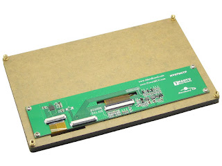
Affordable 7" capacitive touchscreen - about $32 


Character Building Stuff


Neo-Retro Computer - Interchangeable with £10 note.

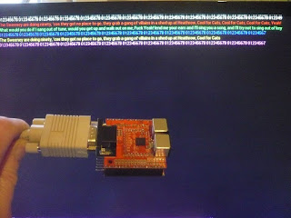
One area of of development of my Neo-Retro computer that has been in a holding pattern for the last few months is the graphical user interface, or GUI.  You may recall that over Christmas and New Year, I experimented with the FT812 graphics coprocessor device, normally intended for driving LCDs - but with a little bit of hardware bodgery (24 resistors)  - it can be made to generate a VGA display for a widescreen monitor. 

The FT812 is about $8.80 in 1 off quantities and requires very little other than a crystal and a few passives to generate the VGA output.  It connects to the mcu via the SPI bus plus a couple of control signals.

1024 x 768 colour text from the FT812 and ATmega1284
It provides a neat and low cost means to get quality video output from even the most resource strapped microcontrollers eg Arduino/AVR,  MSP430, Teensy etc.

If you can't Make - Simulate!

FTDI provide a simulator application (download for Windows) that allows you to develop GUI screens on a Windows PC. Very quickly you can build up the various graphical components and "widgets" into the display list (DL), that are typical on a modern LCD based product.

Once you have your display list and the right look, it's then relatively easy to import the DL into your own C code.  For those using Arduino, Discovery F4, Raspberry Pi - there is technical support for this on the FTDI website.

Even a very modest microcontroller can support a Touchscreen GUI using this method, which can be used for LCDs in handheld equipment - or plugged into a large screen monitor for easier viewing.

LCDs are so cheap now - 7" screens with capacitive touch from China are selling for about $32. Or you can buy a ready made screen module 5" diagonal, 800 x 480 pixel resolution complete with FT810 controller, LCD and bezel for $33 or less - all ready to fit to your latest project.

800 x 480 Resolution with FT810 for about $33

Back of console showing various interface connectors

Programming the FT81x

There are several font sizes available, graphics primitves such as lines and points (circles), buttons, sliders, shading effects, clocks, dials and audio samples and effects - which rapidly allow you to build up a full GUI.  Both resistive and capacitive touchscreen technologies are supported - allowing for object selection, swiping, gesturing etc.

Indeed many of these features have been well explored in the GameDuino II product by James Bowman, - a complete retro-gaming platform using the FT8xx embedded video engine and an Arduino. Neither the FT81x datasheet nor Programmers' Guide do real justice to what this clever $8 IC can actually do.  James Bowman's Book on GameDuino 2 describes the capabilities in much greater depth with graphical examples.

Now for some quick screen "experiments".  All of these are achievable with a small microcontroller (MSP430, ATmega, ARM) connected via the SPI bus to an FT81x device.  Suitable dev-boards are available from FTDI, with or without LCD, or the Gameduino 2 is FT800 hardware plus an I2C accelerometer and audio output jack conveniently brought out to Arduino shield compatible pins.

The first shows some 16 lines of text, a shaded background effect and 4 User Buttons.  This can be quickly built up from a series of display list commands by the process of compositing.

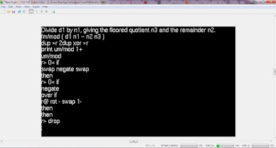
A GUI aimed at displaying Forth Source Code - plus some User Buttons

The only downside of the FT81x is that you are limited to 2048 entries on the display list - and this means only about 2000 characters of text - as each character, with formatting occupies on average just over 1 entry in the display list. However, the screen above with 16 lines of source code and 4 buttons uses 32 for the background shading effect, 300 entries for the text and 228 for the buttons.

However, the whole point of a Graphical User Interface is that it uses graphics rather than just plain text to convey the information.  A picture is worth a thousand words ... literally. And these days, most things can be conveyed in 140 characters or fewer.....

Just the Forth source code

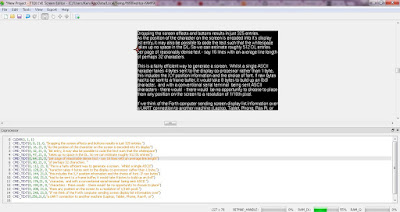
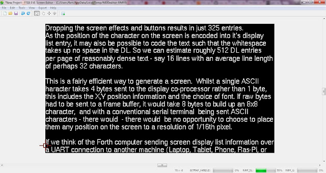
Dropping the screen effects and buttons results in just 325 entries. As the position of the character on the screen is encoded into it's display list entry, it may also be possible to code the text such that the whitespace takes up no space in the DL. So we can estimate roughly 512 DL entries per page of "reasonably dense" text - say 16 lines with an average line length of perhaps 32 characters.

This is a fairly efficient way to generate a screen.  Whilst a single ASCII character takes 4 bytes sent to the display co-processor rather than 1 byte, this includes the X,Y position information and the choice of font. If raw bytes had to be sent to a frame buffer, it would take 8 bytes to build up an 8x8 character, and with a conventional serial terminal  being sent ASCII characters - there would be no opportunity to choose to place them any position on the screen to a resolution of 1/16th pixel.

Fairly Dense Text and Display List 55% used
Just the text: 1062 characters - encoded into 1130 entries in the DL
CLEAR(1, 1, 1)
CMD_TEXT(0, 0, 21, 0,"Dropping the screen effects and buttons results in just 325 entries.")
CMD_TEXT(0, 16, 21, 0,"As the position of the character on the screen is encoded into it's display")
CMD_TEXT(0, 32, 21, 0,"list entry, it may also be possible to code the text such that the whitespace")
CMD_TEXT(0, 47, 21, 0,"takes up no space in the DL. So we can estimate roughly 512 DL entries")
CMD_TEXT(0, 64, 21, 0,"per page of reasonably dense text - say 16 lines with an average line length")
CMD_TEXT(0, 80, 21, 0,"of perhaps 32 characters. "
CMD_TEXT(0, 112, 21, 0,"This is a fairly efficient way to generate a screen. Whilst a single ASCII")
CMD_TEXT(0, 128,21, 0,"haracter takes 4 bytes sent to the display co-processor rather than 1 byte,")
CMD_TEXT(0, 144, 21, 0,"this includes the X,Y position information and the choice of font. If raw bytes")
CMD_TEXT(0, 160, 21,0,"had to be sent to a frame buffer, it would take 8 bytes to build up an 8x8")
CMD_TEXT(0, 176,21, 0,"character, and with a conventional serial terminal being sent ASCII ")
CMD_TEXT(0, 192,21, 0,"characters - there would - there would be no opportunity to choose to place")
CMD_TEXT(0, 208, 21,0,"them any position on the screen to a resolution of 1/16th pixel.")
CMD_TEXT(0, 240, 21,0,"If we think of the Forth computer sending screen display list information over")

CMD_TEXT(0,256,21,0,"a UART connection to another machine (Laptop, Tablet, Phone, Ras-Pi, or")

The sequence of commands in the display list to produce the above screen. Whilst I have manually edited my text to fit into command format needed by the FT810 simulator - this process could easily be automated by the MSP430 - in Forth.

Further Thoughts

If we think of the Forth computer sending screen display list information over a UART connection to another machine (Laptop, Tablet, SmartPhone Ras-Pi, or CHIP) which then renders this information into a user display, then the complete DL of 2048 x 32bit words could be sent in approximately 89mS over a 921600 baud serial link. This would allow typing and editing of text in real time - for most humans.

The FT81x device provides on chip support for resistive or capacitive touchscreens - so that positional information of touches, swipes and gestures may be gathered.  On a widescreen implementation, it would be a relatively simple method to create a mouse cursor - and use this for text highlighting, object selection, and invoking common user commands.

Forth is approaching 50 - and so it really is time to move away from purely text based input.  The GUI can offer so much more including command mapping, colour, highlighting - plus perhaps some of the user interface features that the SmartPhone Generation (anyone under 8) will expect. The FT81x series of ICs offers a really cost effective means of achieving or at least experimenting with these ideas.


The simulator allows you to quickly and easily build up various GUI screens 
In the next part I will further some of the user interface ideas, in ways designed to minimise typing and maximise the features of the Forth Language.

As the SPI interface and control lines between the mcu and the FT812 is just 6 wires plus power, it's fairly easy to hook up to your favourite micro on a breadboard.  Hopefully in a few days I will have the FT812 wired up to ChipStick and be able to generate these screens for real.  I've been there already with Arduino based hardware - so now it's time for the MSP430 FRAM devices.   8 jumper wires and a LaunchPad should be all that's needed.

In the meantime - if you wish to experiment with the FTDI FT81x Display Simulator application - you can download it from here.

You may also be interested in the othe recent posts on ChipStick

ChipStick - A Diminutive Dev Board

The $5 Forth Computer

First Steps to Building the $5 Computer

Digital Dust

Constructional Guide

Bootloader

Interfacing Memory

I/O Expansion

Graphical User Interface

Applications


ChipStick - I/O Magic!

$
0
0
Project Update

First a few words about the current status of the ChipStick project.

This week, the first of the prototype ChipSticks have been sent out to the "Early Adopters" - those with the skills and experience to port Forth onto the device - and thereby "hit the ground - running".

I have also spent some time working on the method for bootloading the device using the CH340G USB comm port and a PC BSL Scripter tool. This is now working on a modified prototype board, and these mods will either be handled with a board revision or some change to the available scripting tools.

I/O! 

When I first devised SIMPL - as an extension to Txtzyme, I believed it to be a great means to improve the quality of interaction between the User and the embedded device, especially when coupled with some interactive hardware such as LED arrays and switches.

Within a few days of the first version of SIMPL, I was connecting it up to LED arrays, and devising a user word "n" which would display the number in binary on a LED array.

Learning by Fun!

ChipStick is all about having fun learning about electronics and computing - so that's why it comes with some preprogrammed words to allow LED displays and musical tone generation to be explored. ChipStick's hardware has been made as versatile as possible, with the aim of future expansion.

Digital outputs are connected to Port 2 and numbered 0 to 7, and each may be connected to a LED via a suitable (270R) resistor.  With this it is possible to turn on individual LEDs, or to have them display an 8 bit binary number.

In it's basic configuration, an array of up to 8 LEDs can be supported and three push switches.

With the addition of some extra hardware, an 8x8 LED array or a 32 key keyboard can be used.

Shift Registers

Shift Registers are the key to economic expansion of the hardware. They are ideally suited to the SPI bus environment and can handle reasonably high speed transfers or data both out of and into the mcu.

The 74HC595 is a serial to parallel converter, costing around $0.10 in volume and ideal for driving LED arrays and keyboard scan lines. The 74HC165 provides the complementary function of parallel to series conversion - and is great for scanning key matrices and arrays of digital inputs.

During this week, I had a little success getting an array of 7 LEDs to mimic the stack operations and one upcoming project will be to use a pair of external 74HC595 shift registers to extend these LED arrays to extend the stack viewer to the full 16 bit.

I have already made a start on this by digging out the hardware used on my "shift register" breadboard - first used back in 2014 for my "A Little Bit Shifty" blog post, where I explored the use of shift registers for input, output and driving stepper motors. This board allows an additional 16 output bits to drive LEDs and 16 input bits from switches. This makes it possible to use ChipStick to recreate 60's style Retro Computers - similar to the Kenbakuino.

ChipStick gains additional 16 Inputs and 16 Outputs using Shift Registers

It's great to see the effect on the LEDs following stack arithmetic and logic operations - a wonderful, visual and interactive way to learn binary arithmetic and boolean logic.

Memorable Events

Last weekend, I had the opportunity to catch up with writing some new firmware functions to get the 128K memory working, so now most of the pieces of the "Forth Computer" are starting to fall into place.

The remaining parts still to work on are the code that will interface to PS2 kepboard and mouse, and of course tying in the system hardware with the FT812 embedded video engine hardware.

This has just become the subject of a recent post.


ChipStick - Initial Orders

$
0
0
When the team at Cambridge got the EDSAC digital stored program computer to first run on May 6th 1949 - it was a major leap forward for the fledgling British computer scientists.

The "Initial Orders" were effectively a bootloader - which was entered into the memory store, electro-mechanically using preset uniselectors - a bit like dialling the numbers in,  with an old rotary dial telephone. Once loaded into the first 30 or so locations of the store, it would run a small program to allow the main program to be loaded from a punched paper tape.

For those interested in early computer history - the University of Cambridge Computing Laboratory have produced a commemorative poster - detailing the Initial orders, the instruction set and operation of a Squares Program running on the EDSAC machine.

EDSAC - University of Cambridge 1949

ChipStick  - 67 years on - still needs "Initial Orders"
ChipStick, if you can summarise it in a few words, is basically a very small, 16-bit microcontroller based, I/O device dev-board on the end of a USB cable.

The USB connection provides communication, power and the means to program new code into the microcontroller.

ChipStick measures just 40mm x 11mm yet meets or exceeds many of the capabilities of the Arduino, some 7 times its board size.

In order to develop code on this platform, we use an interpreted language - Forth, and so the host computer need only send a few ASCII command strings to the device, in order to control it.

ChipStick Goes Forth!

A first batch of 20 band built ChipSticks were distributed to some eager "early adopters".  Within a few days of receiving the pcbs - we had a version of Forth ported across to the FRAM based MSP430FR2433 microcontroller.

ChipStick places a strong emphasis on programming interactivity. For this reason it offers native Forth language, as standard, allowing immediate interaction with the application code.

For more details on the Forth implementation, see the Mecrisp site.


ChipStick being used to help debug some SPI RAM issues
ChipStick offers up to 16 I/O lines, of which 2 are generally kept for serial communications to the PC.

Up to 8 LEDs may be driven as an array, for immediate interaction with the application.

ChipStick is intended to be a low cost experimental and educational device. The combination of a moderately fast 16 bit processor, ferro-electric non-volatile memory (FRAM) and three separate fully function communications interfaces make it a versatile device. Additional SPI peripherals may be added including extra RAM or FRAM, shift registers for Input and Output, motor drivers, high resolution ADCs, DACs, temperature and pressure transducers, accelerometers, gyroscopes, compasses etc. In fact ChipStick can interface to virtually any device that has SPI, I2C or UART interface.

ChipStick has 15.5kBytes of FRAM available plus 4kBytes of SRAM. Whilst this may seem small by some standards it is more than enough for most sensing or control tasks.  Additional memory for data storage can be added using the SPI Port B.

Communications Interfaces

ChipStick is based on the newly available MSP430FR2433 microcontroller, but the pcb can also accept similar MSP430 devices from the FR25xx and FR26xx series - which are aimed more specifically at capacitive touch sensing applications.

It features three separate enhanced Universal Serial Communications Interfaces (eUSCIs)  which can provide a mix of UART, IRDA SPI and I2C interfaces.

Two A type eUSCIs provide UART, IRDA and SPI capability.

One type B eUSCI provides SPI and I2C capability.


                   +------U------+
1             3V3  |  CHIPSTICK  | 0v                20
2             P3.2 |             | P2.1 XIN          19
3      PC-RX  P1.5 |             | P2.0 XOUT         18
4      PC-TX  P1.4 |             | TEST/SBWTXK       17
5  UCA0 CLK   P1.6 |             | /RST/NMI/SBWTDIO  16
6             P2.3 |             | UCA1 MOSI         15
7  RAM_/CS    P3.0 |             | UCA1 MISO         14
8  UCB0 STE   P1.0 |             | UCA1 CLK          13
9  UCB0 SCK   P1.1 |             | P2.3              12
10 UCB0 MOSI  P1.2 |             | P1.3 UCB0 MISO    11
                   +-------------+

                   +------U------+
P3.0  /CE          |   23LC1024  | 3V3
P1.3  MISO         |             | HOLD - pull up to 3V3
      NC           |             | SCK  - P1.1
      0V           |             | MOSI - P1.2
                   +-------------+

The diagrams above show the pin-out of ChipStick - and also that of the 128K bytes 23LC1024 SRAM that is located on the underside of the pcb.

Programming and debugging the initial code image of Forth  is done with the aid of an MSP430FR4133 Launchpad.  The jumper links are removed from the FET connector, allowing jumper wires to be connected from TEST and /RESET to the SBW pins on the dual row header.

Once Forth is loaded - it takes over and allows the full interactive programming of the standalone ChipStick by way of the USB to Serial adaptor - built into the end of the pcb.


You may also be interested in the other recent posts on ChipStick


ChipStick - A Diminutive Dev Board

The $5 Forth Computer

First Steps to Building the $5 Computer

Digital Dust

Constructional Guide

Bootloader

Interfacing Memory

I/O Expansion

Graphical User Interface

Applications


ChipStick - A Small Scale Experimental Forth Machine - First Forth!

$
0
0


Two weeks ago, I introduced a new project, ChipStick - a small dev-board based on the MSP430FR2433 16-bit microcontroller.

The aim of ChipStick is to provide interactive programmable Smart hardware to bring your next project to life.

Late last night I received from Matthias Koch - the first draft of Mecrisp 2.03 Forth ported especially for the ChipStick.

I am please to announce that when loaded into the ferro-electric memory of the ChipStick that it burst into life and was immediately recognisable as a full-blown Forth System.

Forth provides the ideal interactive development tool to help breathe the life into your latest hardware.


Historical Note

Forth was developed in the late 1960s by Charles H. Moore, whilst working with radio telescopes, controlled to minicomputers.

There are numerous online documents describing the history of Forth - so I shall not go into too much detail - needless to say, that Charles "Chuck" Moore wanted a more efficient programming environment and wanted to have control over the whole system.

Forth became popular in the late 1970's - with the 8-bit microprocessor revolution. It offered an alternative to machine language and was well suited to the resource limited systems of those times - often fitting into 4Kbytes or less.

Needless to say , Forth is a very compact and versatile language - and a very good fit for the modern 16-bit and 32-bit microcontrollers. The Mecrisp implementation is about 11k bytes of FRAM.  On the MSP430FR2433 that leaves 4K of FRAM and 4K of SRAM for the Users application code.  There is also the 0.5kB Info RAM - which can be set as a protected area.

Using Forth

Forth uses natural language words, separated by whitespace.  Forth source code may be composed using nothing more than a text editor and uploaded to the target using a terminal program - such as Termite or TerraTerm.

Forth uses 16-bit integer maths as standard - though there are extensions for floating point. However integer math is not so much of a limitation  355 / 113  can be more useful than you think!

Forth consists of a dictionary of standard words, to which the user may add their own new definitions of words.

Any high level control can be broken down into a series of  smaller operations - for example a control cycle for a washing machine.

CHECK_DOOR
FILL
HEAT
CHURN
DRAIN
FILL
RINSE
DRAIN
SPIN
BEEP

Obviously there would be some decision making logic connecting these tasks,  and the CHURN cycle, and RINSE, DRAIN SPIN cycles may be repeated a number of times depending on the type of wash required - but it illustrates the point of reducing the problem to a series of self-contained tasks.

Once the problem has be thus decimated, the high level tasks may be written in Forth, using whatever native language is appropriate to the tongue of the user. If you want to use German, French or Mandarin for the high level names - that is perfectly acceptable.

Forth needs to have a good relationship with the register level hardware of the chosen microcontroller - and the closer to the actual microcontroller peripherals you can get - the more versatile Forth becomes.

It is fairly straight forward to define simple words that allow you to exercise the GPIO.  A quick look at the MSP430 datasheet -and you can construct these new words in a few minutes.  Additional words would be constructed for setting timers, reading ADCs, SPI, I2C transfers to displays or external devices plus anything else of the myriad of operations you might wish to do with the hardware.

Note how all these word definitions start with a colon : and end with a semicolon - this gives them the name "Colon Definitions"

Once entered into the dictionary - these new words are ready and available to use as you like, or combine to make larger words.

Setting the ports

: P1IN  512 C@ ;
: P1OUT 514 c! ;
: P1DIR 516 c! ;

: P2IN  513 C@ ;
: P2OUT 515 c! ;
: P2DIR 517 c! ;

: P3IN  544 C@ ;
: P3OUT 546 c! ;
: P3DIR 548 c! ;

Lighting LEDs on Port 2

: P2LEDSET 255 517 c! ;    (set all Port 2 pins to output)
: LEDNUM 515 C! ;          ( display a binary number on LEDs)

Onboard LED on Port 3.1

: LEDON 2 P3OUT ;
: LEDOFF 0 P3OUT ;

Dump the FRAM in HEX base

: hexdump hex c400 c800 do I c@ . space loop ;
: texdump hex c400 c800 do I c@ emit loop ;

Once you have these definitions store in memory, you can type  170 LEDNUM - and turn alternate LEDs on your LED array.

To be continued.

Meanwwhile  - If you want to catch up on previous ChipStick posts - have a look at the links below:


Adventures in Forth Land

$
0
0
This week, Matthias Koch sent me the files for his Mecrisp Forth MSP430 -  ported specially across to the MSP430FR2433 which is used on ChipStick.

In this post - something of a tutorial, we look at the basic steps needed to get your minimum Forth system up and running, which means loading and executing Forth source code. Fortunately we do not need a whole bunch of special tools work with Forth - as Forth has much of this functionality built in, editor, compiler, interpreter.

In order to program ChipStick effectively with Forth, load, save and edit source code, you will need the following:

  1. A terminal program capable of sending a text file.
  2. A text editor - such as NotePad++
  3. A breadboard with some LEDs - plus any other hardware you want to interact with

For Windows - the terminal I can recommend is TeraTerm - as it has a very flexible scripting language to allow you to customise the terminal operations.

For Linux there has been especially written  e4thcom, which comes with many additional features incuding a GTK+ GUI called ForthBox. There are comprehensive instructions here with the download  -  e4thcom - A Terminal for Embedded Forth Systems

For MAC OSX - working under Homebrew - you can use PicoCom.  

To install PicoCom on MAC OSX with Homebrew, enter this in a command shell: 


brew install picocom


As I am more familiar with Windows, the rest of this tutorial will look at working with TeraTerm.

Serial Set-Up

ChipStick running Mecrisp uses 115200, 8, N, 1 serial communications - but if you are using TeraTerm you first have to set up a macro - that inverts the DTR and RTS lines.  The reason for this is that with RTS low - the MSP430 is held in reset - so Forth will not run!

Equally, togging RTS, with DTR high will perform a hardware reset of the MSP430 - if you really get stuck in a jam.


Inverting RTS and DTR is done with the following lines 6 of code which we save in TeraTerm as a script text file.

; enable dtr
setdtr 1
; clear rts
setrts 0
; now clear dtr, so that the system will reset and see rts clear
setdtr 0

Save these as a file  "mecrisp_reset.ttl"  in the root directory of TeraTerm.  TTL is the filename extension given to the TeraTerm scripting language.

Open up TeraTerm, selecting serial and which ever port the ChipStick's CH340 has connected to- and under the Set Up menu tab - set the terminal options as follows:


Setting up the serial com port parameters

Note the 50mS delay at the end of each line - this gives the Mecrisp Forth interpreter sufficient time to compile each line of source code and answerback "ok." You may choose to vary this delay to between 10mS and  50mS- depending on your system.  If you make th delay too short, some long lines will not be compiled - so I found 50mS to be a safe compromise.

Later, at the end of this post, I will introduce a more sophisticated TeraTerm script that further automates the file sending - and intelligently waits for the "ok." prompt at the end of each line. See end of post for details.

Next - under the "Control" menu select Macro, and then navigate to where you saved the Mecrisp macro - that inverts DTR and RTS


Select the "mecrisp_reset" macro

Once you have sent this macro, the Mecrisp Forth should reply with 

Mecrisp 2.0.3 for MSP430FR2433 by Matthias Koch

and hitting return a few times should give you the usual ok. prompt.

Now we want to send a few Forth words to the target - to set up the GPIO for simple input and output commands

Here is the text we will send:

: P1IN  512 c@ ;
: P1OUT 514 c! ;
: P1DIR 516 c! ;

: P2IN  513 c@ ;
: P2OUT 515 c! ;
: P2DIR 517 c! ;

: P3IN  544 c@ ;
: P3OUT 546 c! ;
: P3DIR 548 c! ;

: P2LEDSET 255 517 c! ;    
: LEDNUM 515 c! ;         

: LEDON 2 P3OUT ;
: LEDOFF 0 P3OUT ;

P2LEDSET
170 LEDNUM

Using a text editor, copy this text and create a text file called chipstick_init.4th

This can also be saved for the moment in the TeraTerm root directory

The first nine definitions just allow us to write values into the GPIO registers, or read the state of the input pins.

For purposes of introduction, I have chosen to make all of Port 2 an output port, with LEDs connected via 270 ohm resistors - see photo:


The P2LEDSET word just sets all of the Port 2 lines to outputs.

LEDNUM takes an 8 bit word off the stack and sends it to Port 2 - thus causing the LEDs to light up according to the binary number value sent.

LEDON and LEDOFF alow the single, user LED on P3.1 to be turned on and off.

The last two lines of the file are immediate operations, to be executed as soon as the file is loaded.  P2LEDSET will make all of Port 2 outputs, and 170 LEDNUM will set the LEDs to an alternate on-off pattern - as 170 or AA in hex is binary 10101010.

We now send this file to the ChipStick, by selecting the Send File option from the File menu on TeraTerm.  Select the chipstick_init.4th file that you saved earlier and press send.

It will be sent line by line to the ChipStick - which will respond with ok. as each line of source code is compiled into memory.

The process takes under 1 second - and you can then use "words" to see that the new definitions have been added to the dictionary.

If all is well you should see this:


The new word definitions are now in the dictionary - and you are free to use them as you wish:

63 LEDNUM  will light up the bottom 6 LEDS

you can even try small binary arithmetical or logical operations and display the results on the array of LEDS

6 7 + LEDNUM

Mecrisp Forth is not case sensitive - so lednum and LEDNUM are the same word.


An Improved Uploader Script.

If you are using TeraTerm, you can take advantage of Jean Jonenthal's Teraterm Mecrisp Upload Helper script that speeds up the source code transfer, by actively detecting the ok. prompts from the compiler before sending the next line of source code. This allows the transfer to run at the full baudrate - without the need for the line delays - which may be up to 50mS.

In addition to removing the need for line delays, the script ignores comments in the source code and also recognises the word "include" so that other source code files can be added in.  It is very useful for uploading larger projects with source code across several files.

The script may be found here via github

Save this .ttl file into the root directory of TeraTerm.  When you want to upload a source file to the ChipStick, you run this script as a macro.  It prompts you for the filename of your source and confirms that you want to send.

Next Time


In the next posting we look at the use of the SPI bus and using shift registers to extend the I/O capability.


If you wish to catch up on the series of Chipstick posts - you can find them from these links:

ChipStick - A Diminutive Dev Board

The $5 Forth Computer

First Steps to Building the $5 Computer

Digital Dust

Constructional Guide

Bootloader

Interfacing Memory

I/O Expansion

Graphical User Interface

Applications


More Distractions of the Mind - Building Retro Computers - Part 1

$
0
0
I2C Hex Keypad & 8 digit Display - about $2.50

Early computers traditionally had rows of indicator lamps to show the state of their registers.  This allowed the service engineer at a glance to check that a program was running, and by single stepping through the code, one could see the effect that the instructions had on, for example, the contents of the accumulator. For low level debugging and diagnostics, a row of LEDs takes some beating.

PDP-8 Front Panel - Indicator Lamps - from about 1965

However, it's about 40+ years since LEDs were fitted to the front panel of mini and microcomputers - which makes them somewhat novel these days.

As a proponent of the Neo-Retro, I set about investigating ways in which LEDs could make a comeback.

The iconic Altair 8800 - from 1975

There are already some fantastic devices out there that use LEDs to great visual effect - such as RGB matrix tiles, POV displays and 3D LED cubes.  A trawl of YouTube reveals some wonderful creations. However, lets start at the beginning and look at the illuminating relationship between computer memory and LEDs.

Shift Registers

Starting with the humble shift register - for example the inexpensive 74HC595, one of the simplest forms of memory. A string of 8 D-type flip-flops connected in series.  As the clock signal rises, whatever the state of the serial input pin at the clock transistion, is copied into the first D-type of the chain. At the same time, the output of the first D-type is copied to the 2nd stage and so on. After 8 clock pulses, all of the D-types have refreshed data, and the previous data held in the register has been clocked out of /H pin.  The diagram below illustrates this in a 4 bit shift register.

shift register
4 bit Shift Register - Internal Workings

It's taken me 5 sentences and half a lifetime, to discover and describe the elegance of the shift register. It has a low transistor count and this made it popular amongst the early computer designers.  With 74HC devices, the clock can reach the order of 100MHz - plenty fast enough for most purposes.

Shift registers are cheap - as low as around  $0.05.  Though compared to other forms of memory - this is a very high cost per bit!

The 74HC595 has the advantage of a separate 8 bit storage register, so that previous results can be held in the register, whilst other data is being clocked through.  This storage function is very useful when cascading registers, in applications such as driving RGB LED arrays.

So we have an easy to use, versatile storage element, onto which we can connect some LEDs, and we can drive it with simple bit-banged port pin output routines, or use a dedicated SPI interface.

From Paul's Electronics - wiring LEDs to 74HC595 

So on a  breadboard, we can put a shift register, 8 LEDs with current limiting resistors and start to write light sequencer patterns to the LEDs. But wait, the illuminated LEDs are only mimicking the value of the bit pattern stored in the register - so at a glance we can read the value of the data held in the storage register.

Now if we had a bunch of registers, and enough LEDs, we could set up a series of LED arrays, and use these to show the data contained in certain internal registers within the processor. Fortunately for us, there has been a small revolution going on with LEDs - and they are one of the cheapest components on the planet.  There are also some really innovative ways of packaging and driving LEDs - which makes them so much more fun - very low cost and much simpler to use.

7 Segment Displays

These have been around for about 50 years - and were certainly used to effect on the 1965 Apollo Guidance Computer DisKey unit- but not necessarily using LED technology.  They are now ridiculously cheap and available in a wide variety of colours, sizes and digit configurations.

Apollo Guidance Computer DisKey Unit - using 7 segment displays

Red is the most common colour, but green, orange, yellow blue and even white are also available.

Size refers to the visible height of the illuminated digit - available from about 2.5mm to 125mm (0.1" to 5").  Some large outdoor displays - such as fuel signs at filling stations and public clocks also use a 7-segment arrangement - sometimes LED or lamp, but also using solenoid driven reflective flaps - that appear either light or dark.

Traditionally the segments are arranged in an "8" shape and given a specific naming convention - called by lower case letters a to g.  The decimal point, if available, is often labelled as dp.

Digits are available as single units or in multiples of 2, 3 and 4 (possibly 5) - and they butt together neatly so you can build up displays of whatever pattern you wish.  The front face of the display is often painted in black - for good contrast and to reduce reflection.  7 segment displays are often placed behind coloured acrylic, masked with screenprint ink - which allows just the digits to show through, with superior contrast - but hides the workings behind.

7 segment displays have been widely forgotten - as they have a much greater power consumption than LCD technology. Allow about 20mA per segment - but remember that though multiplexing it will not be on continuously.

Here are some typical generic 7 segment displays from China.

A Single 0.56" digit - showing size, common cathode (top) and common anode (lower) - about $0.05

4 Digit - 0.56" 7-Segment Display Module - about $0.19
 So why not consider 7-segment displays for your next project, possibly your own miniature Apollo Guidance Computer on an Arduino shield or something quite different - whatever it might be.......

A little inspiration - this time from 1985!
Multiplexing

Fortunately there is a neat trick we can do, so we don't need n shift registers to display n - bits, as this could get quite expensive.  Suppose we have a 7-segment display with segments A to G, with the decimal point (DP).  We connect each of these segments to the outputs of our '595 shift register via current limiting resistors - and with a binary to 7-segment look-up encoded in our firmware, we can display up to 256 patterns of illuminated segments on our digit - of which about 50 might be useful.

If we add another digit, we could just add another 74HC595 to drive that one's segments - however, because of the persistence of vision (POV) we can quickly flash up a digit on display 1, then turn that off, and use the same '595 to drive the segments of the 2nd digit.  7-segment displays are wired internally to allow for this - and are known in the trade as either common anode (CA) or common cathode (CC).

If we have say a display consisting of 8 digits, we connect all the segments to their own "segment drive" output on one 74HC595, and then use another '595 to enable each of the digits in turn  - by pulling down and sinking current out of the common cathode of each digit in turn.  Only 1 digit is illuminated at a time - and for 1/8th of the total display cycle. POV does the rest for us - and it appears that the digits are on all of the time.

The same trick can be applied to the 8x8 LED arrays. One shift register is wired to drive the rows, and the other turns on the columns - in turn. The second shift register is driven with a series of values that only energise one column at a time.  If it is sinking current from a common cathode display it needs the following repetitive pattern:

11111110
11111101
11111011
11110111
11101111
11011111
10111111
01111111

And for common anode - we invert the polarity of the bits so that the register sources current into the common anode:

00000001
00000010
00000100
00001000
00010000
00100000
01000000
10000000

You will notice that these sequences are easily programmed in C using either repeated addition (doubling) or bit-shifting.

So just two of the 74HC575 devices will drive an 8x8 LED array - about $0.20 of hardware.

And For My Next Trick......

There's yet another neat hardware trick that we can do.  We can use the above scan pattern to generate the read sequence required for a keyboard matrix.

Assume that the keys are arranged in an 8 x 8 grid.  We apply the above scan pattern to the rows, ad then use another shift register - this time a 74HC165 wired as a parallel to serial converter,  to read the columns. When a key is pressed, it shorts a row to a column, and so the brief scan pulse appears on the column input of the '165.

In our code, we first write the scan pattern, energise the display segments, then read back the data from the '165 column shift register.  If a key is pressed it will appear as a 1 in a particular bit position of the '165 register.

This is a very economical way to multiplex  7 -segment displays and scan a key matrix. Just two output shift registers and one input register.  It has been in use at least since the mid-1970s - and possibly earlier - applied to vacuum "Nixie" tubes.

Fortunately this functional requirement is very common - for example in cash registers, and machine automation systems - so the function has been integrated into an easy to use IC - available from various manufacturers for a few cents.  Each offers different numbers of display capabilities and keyscan matrix options. Whilst you can drive these from shift registers, there are some really neat, low cost ICs available to make your job a lot easier.  These communicate generally via I2C and are useful for driving either arrays or 7 segment displays. Some also have the means to scan an array of keyswitches. It all makes interfacing to your microcontroller a lot easier.


Display Driver ICs

The Holtek HT1632C is typical of the low cost display driver ICs - and will drive 24 rows by 16 commons.  It's worth a look at the datasheet for full details.  The HT1632C is a ubiquitous IC in the Shenzhen markets - costing around $0.50 in 1 off. It is however available only in a 48 pin or 52 pin LQFP - so you will need a LQFP adaptor to use this in a breadboard.  Having recently paid $8 for a QFN adaptor from the US - I was delighted to see these available in China for around 11 cents!

There are other driver ICs available - from Holtek and other manufacturers.  The HT16K33 will drive up to 128 LEDs and scan up to 39 keyswitches. Conveniently there is a little breakout board available from Adafruit for the 16K33.  It's $6 in the US or under $1 in China for a lovely purple pcb - a rapidly becoming popular colour choice for pcb solder resist.

HT16K33 Breakout - An Adafruit Design - Significantly cost reduced in China!

If you don't have many LEDs to drive - there is the very economical TM1638.  This is about 12 cents and will scan up to 24 keyswitches.  It's available as a built up board containing 7-segment displays and low cost tact switches. It will drive 8 x 7 segment digits plus 16 individual LEDs - all for under $2!
I2C driven TM1638 on a pcb with 8 x 7 segment, 8 LEDs & 8 Switches Yes - that really is $1.86!
The TM1638 has a sister device - the TM1639 that will run 8 x 8 LEDs and scan up to 16 switches - this time in a more breadboard friendly  DIP24 package.  The datasheet in Chinese has suffcient diagrams and English text to allow you to make a good understanding of how it is deployed - including example circuit diagrams.

Another useful part is the TM1628 - It will scan 20 keys and drive up to 10  segment digits - see below


You can but these ICs already fitted to a board complete with 7 segment displays and switches. The innovatively named "LED & KEY" pcb - below, is one example of a fairly generic design - from as little as $2 in the markets.


All of these items were located via TaoBao.com - the Chinese equivalent of Ebay. The TaoBao search engine now recognises English text - and for the reverse translation - let Google translate the page.  So lots of cheap hardware is available - you just need to know where to search online for it!

LED Arrays

For a few tens of cents, you can buy a variety of LED arrays - either with single colour LED,  bi-colour or RGB. These are generally in 8x8 arrays using either 3mm or 5mm LEDs - but there are some using 1.9mm LEDs  - which means a smaller physical size - or more LEDs in a given size package.

Typical Datasheet for a common anode LED array

For, me, the 16x16 array of red LEDs in a 40mm square package holds the greatest potential - and I will look at this later - in the meantime - here's what they look like.

16x16 Red LED Array with change from a $6 bill!


16x16 array - and a HT1632 driver IC - all in one module


Finding the Chinese search term - or the generic name of the part is half the battle. For example, one item of interest is the YK-788BS 1.9mm 8x8 LED array. Adafruit sell these for $3.95 but the market price in Shenzhen is closer to $0.30.  You just need to know that a TaoBao search on 788BS is going to find most of the references to this part.

These miniature 8x8 LED arrays have a 16 pin DIL pinout - so you can breadboard them easily, and stack them side by side on stripboard to make larger arrays.  You could easily construct  a 16x 16 array, with 2 off HT16K33 driver ICs for well under $5. Here are some I bought recently, with the proposed EagleCAD layout below.

Half Size 20mm x 20mm LED Arrays $0.29 each!

8x8 LEDS arranged into a 16x16 LED Array Shield with 2 x HT16K33 drivers ICs
Shopping Around

I do a fair amount of purchasing in and around Shenzhen - so it helps to have contacts over there who understand electronics, understand the language and culture, have local knowledge of the main markets and who can do business on your behalf.

If you want to source components from Shenzhen markets - I recommend Man Friday. They are a relatively new company offering personal shopping for component sourcing and shipping services.
Contact Toby Yu for details - and mention my name, Ken.

Toby has excellent English -  he used to teach English in High School, and will go out of his way to help you with your sourcing and manufacturing logistics, as well as offering Shenzhen meet and greet, factory visits, language translation, business negotiation and overseas shipping.

Daniel Bailey's C88 - A computer with just 8 bytes of memory!

This is a neat project by Daniel Bailey of York Hackerspace. It is loosely based on the Manchester SSEM "Baby" but uses a single 8 x 8 LED matrix to show the entire contents of its 8 byte RAM.
Daniel wanted to build a simple processor  from the ground up using a FPGA.

He illustrates his project here  


Daniel has subsequently sourced a 32 x 32 RGB matrix - and is building a machine replica of the Manchester Baby SSEM.

Whilst Daniel's full colour RGB panels are still quite pricey - they can be found in China for about $30 to $45 and also through Adafruit.

For my experimentation - I will be using a more modest display - based on the 16x16 40mm module - but actually more economically constructed from 4 of the 20mmx 220mm 8x8 788BS modules with 16K33 drivers  These can be arranged quite cheaply to make a 32x 32 array, allowing the Manchester Baby to be simulated - for around $20 of hardware, or to single step through a very small window of code on your latest ARM processor.

With a 32x32 LED array with variable LED brightness control - it may also be possible to recreate an early Baird Televisor - with slowscan mechanically scanned 30 line TV!

The combination of innovative LED array products, low cost, easy to use driver ICs and access to the low cost markets of electronics Shenzhen, has made all of  these devices far more available to hobbyists.  They are now such a cheap and easy solution - that there is now very little reason not to use them in your next project.

In the next part we look at driving the 16x16 LED array - and using it as a unique insight into the inner workings of our retro computer.

Links to Related Topics.

Background on Manchester Baby SSEM


The Windmills of Your Mind...... Part 1

$
0
0
Occasionally, moving within the open hardware circles, you stumble across a really neat bit of technology, affordable, well thought out and well implemented, and you think, yeah - wouldn't it be cool to do something with that. Unfortunately, as is the case with most things, you find yourself too busy to strike whilst the iron is hot and the cool things get left - to cool.

The Parallax Propeller

Well, that was my first reaction when I came across Chip Grasey's Parallax Propeller chip. It's been around for about 10 years now, and it was a hot product when it first came out, and it can still hold it's own against the far more mainstream processors.  It is easy to program with minimum amount of kit, provides video and audio output and has a multitude of purposes.

The IP for the Propeller core, was released to the Open Source Community in August 2014 - with full Verilog source available - so you can take an inexpensive FPGA dev board and create your own devices with the Propeller 1 core.  The core supports a 64K long word address space - and with a suitable FPGA platform - such as the Pepino board by Saanlima Electronics, the Propeller could be emulated at

The architecture though novel, is well thought out and it is a sufficiently powerful platform to warrant being studied in electronics and computing degree courses.

In recent posts, I have remarked about the elegance of the 40 pin DIL package, for it's simplicity, ease of handling, breadboard friendliness - and it is no surprise that the Propeller is available in a 40 pin DIL package. It is also available as a 44 pin LQFP and a 44 pin QFN - for applications where space is tight.  All packages provide an easy to remember, very logical pin-out, which for the 40 pin DIL package very effectively mitigates against the possibility of reverse insertion into the socket.

The minimum hardware set-up is trivial - the IC supports everything that you need for an easy to use, quick to set-up multicore microcontroller.

Propeller is Almost Ready to Fly - Minimum Hardware set-up
Propeller has an interesting architecture, consisting of 8 separate 32 bit cores - known as Cogs. These can be individually allocated to hardware intensive tasks - such as video generation, pwm and waveform synthesis and signal analysis.

Propeller can be programmed in assembly language, or a native bytecode interpreted, high level language called Spin.  Additionally for C programmers there is a Propeller-GCC,  other high level languages include Pascal, BASIC and several versions of Forth.

Propeller ICs may be interconnected using high speed serial communications interfaces to extend to a multi-processor system.

I'm not even going to try to describe the full feature set - for that we have the Propeller Wikipedia entry and the extensive documentation on the Propeller Site - including the User Manual and Datasheet.

The Propeller is available in DIP 40, LQFP-44 and QFN packages.  It is stocked in volume by Digikey and Mouser - starting at around $7.99 in 1 off.


What makes Propeller Interesting?

A novel 32-bit architecture - that is now fully open, and can be implemented using various FPGA platforms.

Innovative, scalable hardware - particularly for on-chip video generation. A new Propeller 2 offers higher speed and more Cogs.

Offers a "1980's micro" on a chip. Provides a singe chip solution for low cost products requiring video, audio, SD card, PS/2 keyboard & mouse.

Extendable to multiprocessor arrays - using high speed comms.

May be used as a companion device to another microcontroller - see Micromite Companion.

The bootloader and bytecode interpreter are written in Propeller assembly language, and could be modified or extended. For example to provide bootup from an SPI device or to extend the bytecode language.


Character Set

The Propeller has a versatile character set - clearly designed with engineering purposes in mind.  A collection of standard ASCII characters, electronic schematic symbols,  timing diagram elements, mathematical symbols and Greek alphabetical characters. The characters occupy 16 x 32 pixels, offering a chunky, though very readable display.  With small additions and some custom characters the Propeller could be used for mathematical report writing, schematic capture (electronic circuit design), digital timing analysis and pcb layout.


In the next part, I put together a 50x50mm pcb to carry the Propeller IC plus VGA output, PS/2 Keyboard and mouse.


New Infrastructure

$
0
0
Creating a new Universal Expansion Board  "UXB-101"

For some months I have been creating new designs using a 50mm x 50mm standard shield format - which adds an extra 8 pins to the familiar Arduino shield, and constrains it to just 50 x 50 mm - for minimum manufacturing cost by some of the Far Eastern pcb manufacturers.

I am currently evaluating several different microcontrollers for various projects I have running at the moment.  Some of these can be done quickly cheaply and easily on a 2 x 2" board - but it only takes one 40 pin DIL or 44 LQFP to swamp the pins availabe on that format.  Increasingly there is the need to access more signals or just put much more circuitry on board. I have been using Arduino and Arduino MEGA for the best part of 5 years - and whilst the "bodged" pin-out sometimes infuriates me - the shield format is simple and easy to work with.

The 50x50 format has worked out well for small designs, but the time has come to extend it - particularly in the requirement of larger pin-count microcontroller and FPGA devices. At the same time I wanted to keep it nominally compatible with Arduino and Arduino MEGA - because of the vast number of shields and other boards that utilise these formats.

So I have added some extra at either end to make a 50mm x 101.5mm board (approx 2" x 4") - that has a much greater pin count and increased area for circuitry. It retains Arduino and MEGA compatibility and provides an additional 26 pins more than the Arduino MEGA format.

The name UXB-101 comes from "Universal Expansion Board" 101mm long and that there are 101 useful signals.

Unfortunately it is not possible to shoehorn this board any tighter to get it to fit onto a 100mm board size - to take advantage of the 10cm special offer from some board houses. However, the 10 off price for this board is $2.30 from PCBway.com.


Details of Pin Out

The board has 6 generic 16 bit ports labelled A to F - these have been derived from the Arduino naming

Port A   Analogue
Port D   Digital

For the Port C and D headers, the following suggestions loosely apply.

Port  C  Communications  (UARTs, SPI, I2C etc)
Port  B  "Buttons"

To which I have added E and F  - which are the additional signals found in the double row header at the end of the pcb.

Ports E and F are ideally suited for bus applications - where large numbers of signals need to be connected between a series of stacked or backplaned boards. Applications might include 16 address and 16 data lines,  R,G, B digital video plus sync & control lines, HDMI data etc.

To accompany these "backplane" connectors, there are 4 "Identity" pins  I0 - I3  - these may be used to connect an eeprom or other means of identifying the shield.  They are located at the very bottom of the 2 row header - in a location not used by the MEGA. They could be used as a board select address - allowing one of 16 boards to be selected in a backplane.

5V and 0V accompany the backplane - and it would be likely that each board would have its own 3V3 regulator to step the 5V down to the required level.

The board has been designed for simplicity and versatility. It maximises the amount of space available for the placement of large packages, and can be used as a stand-alone, stacked or in a backplane type application.


New Universal Expansion Board  "UXB-101"

Applications

This board is large enough to accommodate devices in the order of 144 pins, and for some applications - where 30 lines or more are needed to drive a LCD, or large pin-count FPGA packages - larger devices may be used.

The board is not restricted  to microcontrollers or FPGAs - there are sufficient pins available to host a variety of other devices, such as large SRAMs, video controllers or any ICs that have a high-pin count - and the requirement to break those pins out to a 0.1" user friendly spacing.

The board may be fitted with standard or "extended" 0.1" female headers, and for backplane connection - a right angled 2 row "box" header could be used.

The board can be used with half-size breadboards - such as the SYB-46 or other 270 or 300 tie-point breadboards - which fit neatly between the rows of headers.

Some Proposed Projects

It is relatively straightforward to port any microcontroller breakout board design to this board format.

My STM32F746 based "BoB"design of last Summer is an ideal candidate.  The A, B, C, D, E and F port allocations allow the peripherals to be grouped by function to some extent, rather than by pin number.  So if all the pins of the mcu that support ADC, op-am or comparator function are located on Port A, (Analog),  all of those with timer function are on Port D (Digital),  all of those with UART are on Port C (Communications) - etc - this then makes the board fairly compatible with Arduino shields  - regardless of what microcontroller is used. Remember to make sure that at least one UART, SPI and I2C is located on the "original" Arduino pin allocation - to ensure backwards compatibility.

Here are a few of the Breakouts I have in mind:

ARMduino GIGA  -  An Arduino compatible board using a 216MHz STM32F746 ARM Cortex M7
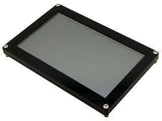
Enterprise              -  A multipurpose board to help teach electronics and computing science. Features LEDs, switches, shift registers etc.

Spartan 6 Breakout   - A breakout board or shield assembly for the popular Xilinx Spartan 6, 144 pin FPGA. Compatible with Gadget Factory's Papilio DUO 

MSP430FR5994 Breakout   - a board to host the new MSP430FR5994 256K FRAM based microcontroller.

Propeller P8X32A Breakout  -  a projects board for the Propeller chip - as discussed in an earlier post.

Gnome -  A multiprocessor experimental machine based on multiple Propeller 1 architecture - either using P8X32A ICs intercommunicating via high speed serial comms - or alternatively implemented using several FPGAs.  Arranged as a "backplane" system - styled loosely on Cray-1.  "A Barbie (and Ken) Sized Supercomputer"

Now that we have a big new, blank canvas, we can start to design some exciting new gadgets.  Later posts will look at the various designs that make direct use of the UXB101.

Whilst the design I have presented is minimal, it can be augmented with extra features such as mounting holes, other permanent features - eg extra components such as LED & reset switch, voltage regulator etc. Then we could use a modified board outline - so as to allow incorporation into other designs.


Handouts and Downloads

Examples schematic and board files of the blank UXB101 pcb created in EagleCAD have been uploaded to my Github Repository


Viewing all 234 articles
Browse latest View live


Latest Images