 |
| myStorm uses a unique low cost approach to provide system integration |
I had been wanting to create an FPGA board for some time - especially now since Clifford Wolf's open source ICE Storm toolset is available.
The opportunity presented itself, when following a discussion with Alan Wood, over a post-OSHUG beer, we decided that we would produce a small FPGA board using the Lattice ICE40HX4K part.
This would hopefully be produced in time for the September OSHCamp - held in Hebden Bridge, near Halifax, Yorkshire.
We wanted a "no-nonsense" FPGA development board that would encourage open source hardware enthusiasts to take their first steps with FPGAs and verilog or VHDL.
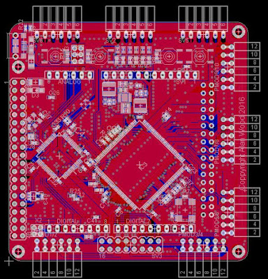
The board had to be 2 layer, fit the size constraints of EagleCAD Lite, and use components that could be soldered at home - by those DIY'ers experienced with Surface Mount parts. For this reason we chose a 144 pin package for the FPGA rather than a BGA - as these are not very friendly either for 2 layer pcb layout, or for soldering.
Alan did the preliminary system design, whilst I looked at finding an efficient means of routing the SRAM to the FPGA for minimum signal skew.
After several Saturday lunctime pub-meetups we settled on an overall design last weekend - that will go for prototyping towards the end of this week.
Low Cost - Achieving a price-point breakthrough!
Seldom do you get much of an FPGA board for under $50 - with the $22 Lattice ICE Stick setting the current lower limit.
But this ICEStick was limited by the HX1K part, and very little accessible I/O. Like a lot of FPGA boards, it also used the FT2232 USB to serial bridge to provide programming and communications, but at around $5, to me has always seemed a rather expensive solution.
Connectivity was a key feature, and so the board uses some old familiar friends - including Arduino "Shield" headers to provide a rich mix of GPIO, 12-bit ADC and communications - including USB, UART, SPI and I2C, as well as providing a large flash array, into which a bitfile could be stored.
The industry standard connector for FPGA dev-boards is the PMOD connector - devised by Digilent - so our board has several of these available.
Finally, another recent ICE40 FPGA board by Olimex has defined a connector for low voltage differential signalling LVDS - and so this 34 pin connector was added as an alternative to the PMODS.
The Olimex board uses a HX1K part which is about $1 cheaper, but we felt that this might be a bit small - so we opted for the HX4K part. Olimex use a 256K x 16 SRAM, and we have stretched this out with an extra address line to allow for 512K x 16 SRAMs.
Some of the design requirements - summarised:
1. Open Source
2. Low cost - suit even the smallest budget - about $30
3. Compact 75x75mm - but with a useful range of signals available
4. An onboard ARM for handling USB comms, GPIO and ADC channels and FPGA loading
5. FPGA should be in an LQFP package - for easier layout and possibility of home assembly
6. A fast 64K x 16 SRAM (512K x16 max) to allow soft core cpu development
7. PMOD and double PMOD connectors
8. Arduino compatible shield headers - giving 5V tolerant GPIO and peripherals
9. A cable or direct connection to Raspberry Pi or Pi Zero
10. A connector to directly drive 32 x 32 RGB LED panels
myStorm is a unique combination Pi Zero, of a fast 32-bit ARM microcontroller and a versatile low power FPGA.
The Raspberry Pi Zero - which hosts all of the FPGA development tools, provides an integrated design environment for FPGA and ARM - aimed at a new concept in hardware hacking projects.
The Lattice ICE40 series FPGA with a large SRAM attached, connected to an ARM M3/M4 Cortex microcontroller provides the ideal platform for developing soft core cpu designs.
The ARM holds the bit-file for the FPGA in flash,
The ARM M3/M4 Cortex provides a USB interface to a PC, plus the following I/O & peripherals:
72MHz/96MHz/108MHz 64 pin ARM Cortex M3/M4 processor:
Arduino compatible with STM32-Duino extension
256Kbytes Flash
32Kbytes SRAM
Up to 37 GPIO lines with 5V tolerance
Up to 10 ADC inputs with 12bit 1MHz ( 2 ADCs)
Three 16bit differential input SD-ADCs (optional)
3 UARTS
2 SPI
2 I2C
Timers
Lattice iCE40HX4K - 144pin LQFP package
Up to 64 I/O lines - arranged on industry standard PMOD ports
Choice of 64K or 512K fast (10nS) SRAM
Can use ICE Studio graphical design environment.
Pi Zero Host Port
Standard Pi 40 pin (2 x 20) GPIO header - allows easy attachment of Pi-Zero for programming and development
Compact 75 x 75mm
ARM Section
Wide assortment of GPIO brought to Arduino shield connectors
6 Analogue Input Lines AN0 - AN5
UART (with bootloader facility) TX, RX
Up to 18 digital lines - including I2C and SPI
Up to 3 differential input 16 bit ADC channels (If STM32F373 fitted)
USB 2.0 connection for programming, data and power
8 bit bidirectional bus interface to FPGA and Pi - Zero with handshaking lines
SPI bus for programming FPGA from bit file
FPGA Section
5 double PMOD connectors
8 bit bidirectional bus to Pi-Zero and ARM
LVDS to "Olimex" style 2 x 16 connector
2 x 8 header for direct connection to 32 x 32 RGB matrix display.
100MHz clock oscillator
64Kx16 fast SRAM
Pi Section
Standard 2 x40 GPIO header for Raspberry Pi GPIO
EEPROM for PIHAT identity
Other
Efficient dual voltage switching regulator
4 USER buttons
5 USER LEDs
RESETswitch
BOOT switch
All I/O on 0.1" grid - wherever possible
Applications.
1. As a stand alone versatile application controller
2. As an advanced Analogue and Digital I/O board for the Raspberry Pi and Pi Zero
3. As a teaching platform for learning 32 bit ARM and FPGA programming.
4. As a platform for developmenting Open Core cpus on the FPGA
5. For high speed digital instrumentation - such as DSO or logic analyser
Cost Reduction
Keeping the cost down was a primary concern, yet we wanted to make a board that was genuinely useful.
To achieve this, Alan came up with a unique strategy:
1. Low cost FPGA with open source tool chain
2. Low cost ARM - to act as "system integrator" and glue.
3. On board Pi Zero - to host the open source FPGA tools - user supplies this at $5.00
Having settled on the ICE40HX4K - as the largest ICE40 available in an LQFP package - and thus more easily routed on a 2 layer board than a BGA part, we set about identifying the other key components.
Having seen James Bowman's J1a Forth Processor - a soft core running in an ICE40HX1K part, I wanted to add a fast (10nS) 16 bit wide SRAM - which in a TSSOP-44 package allows parts between 64K and 512K words. With this combination comes the ability to create a number of soft core processors, of which the 16 bit simple processor described in the "Nand to Tetris" course would seem a very suitable candidate.
Other applications include digital instrumentation that require large arrays of fast memory - such as digital oscilloscopes and logic analysers.
The lynchpin in this design is the use of a low cost ARM device, not only to provide USB communications, storage (in flash) of the FPGA bitfile, plus provide a series of ADCs and 5V tolerant GPIO pins and peripherals to augment the FPGA architecture.
Costing
We believe that if an FPGA board sells for around $30 then it will attract a fair bit of attention.
This was going to be tricky - so we set ourselves a BOM on a very tight budget of arount $10 based around the principal components - costed in 100 and 1000 off quantities:
100 off 1000 off
FPGA $5.56 $5.37
ARM $1.20 $1.00
SRAM $1.69 $1.22
PCB $0.88 $0.49
Connectors $0.50 $0.40
Remainder $0.50 $0.40
Sub Total $10.33 $8.88
LOP $2.58 $2.22
Total $12.91 $11.10
Pi Zero $5.00 $5.00
So in 1000 of quantity, the BOM and manufacturing (LOP = Labour, Operations Profit) comes to a total of around $11, which allows a selling price of about $30.
The customer provides their own Raspberry Pi or Pi Zero, from as little as $5.00.