Quantcast
Channel: Sustainable Suburbia
Viewing all 234 articles
Browse latest View live

The Windmills of your Mind - Part 2

$
0
0
Intrigued by the architecture of the Parallax Propeller IC - which I discussed last week, I decided to bag a couple of dev-boards and have a go for myself.

I must say - that the more I read about this device, and explore the wide variety of uses that others have found for it, the more enthusiastic I feel for it.

It's not an ARM, or an AVR or a PIC - it's something fundamentally quite different.  It has humble beginnings, but appear to be able to punch above it's weight.  It consists of a combination of 8 individual 32 bit processors arranged around a central servicing hub, each with local memory - fast SRAM, and the means to communicate through the central hub RAM.


Mastering the techniques of the Propeller, will give the novice a much greater understanding of how firmware and hardware can interact in a very positive manner  - to create a system building component - that appears to exceed than the sum of its parts.

Having spent the best part of 2 years designing ARM processors into products, I am very aware of the ever increasing complexity of modern microcontrollers. Approximately half of my code is devoted to setting up the peripherals, so that they do what the application demands.  Just flashing an LED on an ARM Cortex M4, takes about 10K of code, and about a week to reach that magic blink moment - from a standing start.

The tool chains to support these chips are becoming monsters - multi-gigabyte behemoths, that take a long time to master. Nothing is quick nor easy anymore - that's why,  when I re-stumbled across Parallax's Propeller (after some years) I was pleasantly surprised.

My Aims:
  1. Learn more about the Propeller and the means of controlling external hardware using it's "soft peripherals".
  2. Create a dev-board that can be applied to a number of projects - complete with a supporting infrastructure
  3. Explore the use of the on-chip VGA video generation, as a means of creating a sef-hosting,  more intuitive user interface - to improve my programming productivity.
  4. Re-visit Forth - either PropForth or Tachyon Forth - as a language for Hardware Exploration
  5. Apply this new software/hardware mix to solving everyday engineering problems.
Parallax are working on a new Propeller IC - which is currently available only as a verilog design that will run on an FPGA.  It appears to increase the performance of the existing design by a factor of about 8. When it makes it's commercial debut, I shall be ready, prepared and waiting for it.

If everything else fails - and 32 bit processor performance plateaus in the next few years, preventing the relentless rise in complexity of the mobile devices we now use, we can re-invent it all - with a big bucket of Propeller chips!


Gimme Hardware 

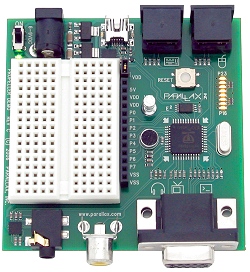
The longest journey begins with the first step - and in this case that step was to source some suitable hardware, at fairly short notice  - and get experimenting.  Unfortunately, in the UK there are not many distributors who carry the Propeller device - but I did find Pimoroni in Sheffield, who have a board called a Propeller HAT intended to be mounted on top of a Raspberry Pi - available for a modest £15 each.

Propeller HAT (underside) - neat pcb in black solder-resist and gold flash
As can be seen from the photo, the Propeller Hat is a fairly simple circuit consisting of the Propeller P8X32A, a small EEprom (24LC32) a 6MHz crystal and a 3.3V regulator.

On the top side of the HAT, running parallel to the long sides of the pcb, there are  two 20 pin headers that break out the pins from the Propeller IC - all except P30 and P31 that are used for the serial interface.

Along the short sides of the pcb, are 12 pin female header sockets - which connect to various pins on the Pi GPIO connector.   In the centre is an area intended to take a self-adhesive mini-breadboard.

Making it Work

Unfortunately, there is a little bit of preparatory work to do before this becomes a general purpose Propeller 1 dev board, rather than a Pi specific one - as the eeprom is actually intended to be the identity eeprom for the HAT, and is not actually connected to the pins of the Propeller IC - doh!

Additionally the 24LC32 is way too small for the Propeller applications  - so the first job was to replace it with a 24LC256 - which fortunately I had available - left over from another job.

The following pins need to be linked before the Propeller will work as a stand alone.

EEprom Vcc  (Pin 8)   to 3V
EEprom  WP  (Pin 6 )   to 0V
EEprom SCL   (Pi Connector pin 28) to Propeller A28
EEprom SDA   (Pi Connector pin  27) to Propeller A29

The using an FTDI cable or similar USB to Serial adaptor

Pin 1   0V   GND
Pin 2   Not connected
Pin 3   +5V
Pin 4   Tx  to Pi Connector pin 8
Pin 5   Rx  to Pi Connector pin 10
Pin 6   DTR

Pi  GPIO Connector - as viewed from above "through the board"


It should be noted that DTR is normally low - and this will cause the Propeller to be held in Reset. (This confused me for quite a while!)  It is therefore necessary to invert DTR with an NPN transistor before connecting to Propeller Reset.

To make up for the missing Raspberry Pi, I used one of my Piano Forte pcbs to act as a base board for the Propeller Hat.  This provides power and a connection point for the FTDI cable, but also has footprints to accept 3 different wireless modules, a micro SD card socket and a Lithium battery boost and charge circuit. Whilst modifying the Propeller HAT was a minor inconvenience, it it more than made up for by the rapid access to a whole bunch of useful peripheral devices. The Piano Forte board also provides an Arduino Shield header format - allowing the Propeller to access all of the Arduino ecosystem too!


Four wires are needed to hook up the EEprom - see text

A  spare, bare, Piano Forte pcb provides power, comms and peripherals
Finally, it's time to play Propeller Pirates!

Parallax has traditionally had a long history with microcontroller educational projects - beginning many years ago with the BASIC Stamp.  This tradition continued when the Propeller took over about 10 years ago with some well thought out kits and starter boards - aimed squarely at educating the newcomer about the unique language and interfacing techniques made possible with the Propeller.

With just a dozen or so resistors, the Propeller can generate VGA video and host a PS/2 Keyboard and Mouse - with this you have the basis of a complete mini-workstation, capable of running interactive BASIC or Forth, or providing the User Interface for other products.

Whilst searching for UK Propeller boards, I also found a rather neat application for the Propeller IC - as a serial controlled VGA generator - illustrated nicely in this video by HobbyTronix.

Propeller has been used for some fairly serious hardware projects.  It is not a toy by any means, and it's ability to use software defined peripherals - make it virtually a unique device.

Several Propellers may be interconnected to form a more complex system, with the peripheral functions shared amongst them.  There is a product called Tri Blade - that contains 3 Propeller ICs - and 1Mbyte of 55nS SRAM.  One propeler handles VGA, keyboards and mouse, another is the main compute engine, and the third is dedicated for interfacing wit external devices - such as ethernet controllers etc.

Some of these boards - often built by interested enthusiasts - feature strongly on the Propeller forum

Here is  a mini board  P8XBlade 2 - by very creative forum member Cluso (Ray Rodrick).

Why I Like the Propeller

I've only been looking at the Propeller chip for about a week now, but already I am starting to like it - for a whole variety of reasons - some from the heart and some from the head.  Here's just a few of those reasons, so far....

The Propeller concept is almost entirely the work of one very talented engineer, Chip Grasey.  Whilst most ICs are these days designed and implemented by a team of engineers - with a multi-million dollar budget, Propeller was developed by Chip aided by a group of friends and co-workers.

Propeller has some very flexible hardware, in the form of counters, which can be used to create a variety of peripheral functions, assisted by some fairly tightly coded assembly language program modules.

The 40 pin DIL version is very easy to prototype with on stripboard, breadboard or perfboard.  As all pins can be allocated to any function, there are no restrictions on what you can connect to what.   Reversing the bus order, or swapping Rx and Tx pins on UARTS becomes simple - just change the code. This is as close as we get to soft-hardware!

Propeller is scalable - more Propeller chips can be added to extend the functionality of a design. PropForth comes with a library that allows high speed communication between Propeller chips. Here's one example of TetraProp - four Propeller ICs on a small board - all talking to a master device with micro SD card.

TetraProp - Four Propeller ICs on top, and another Master IC below


There is a strong community and forum behind Propeller.  Chip Grasey is a regular contributor and treats his customers as friends and co-developers.

The Propeller Tool is by today's tool chain standards a fairly small program.  The executable has a disk image size of just 4Mbytes,  and the whole package, of tool, examples and documentation is about 35Mbytes.

The IP behind the Propeller IC has been open-sourced. You can study every detail, modify and create your own variations which will run within an FPGA.

The open core and multi-processor design of the Propeller IC lends itself to demonstrating the fundamentals of digital microelectronics and microprocessor architecture, and is a perfect platform for studying electronics and computing science at undergraduate level, with sufficient content to encourage creative development.

An article - originally written for RS Components by William G. Marshall - about 6 years ago - captures succinctly some of the key aspects of propeller.

Incidentally, RS Components stock Propeller devices! - both DIL-40 and 44 pin LQFP  - this is good to see that at least one of the big UK/Global Distributors is still supporting these devices.

Next Time

In the next part of this series, I will hopefully have had a chance to play with various aspects of the Propeller, had a look at Tachyon Forth, and will have some peripherals including VGA, keyboard and mouse wired up to the board.

I am not planning to write a book on this processor - that has already been done elsewhere by skilled users. I am just hoping that the information I offer here is sufficient to encourage others to have a fresh look at this fascinating device.


FT812 pcb provides pin connectors for VGA , PS/2 Keyboard and Mouse 


A broad outline of future blog-posts in the pipeline would be (subject to change).

Interfacing VGA, Keyboard and Mouse to Propeller IC using Evita pcb - above

Tachyon Forth

Basic Peripherals - GPIO, SPI, I2C, UARTS, ADC, DAC, Audio

microSD Card


The Windmills of Your Mind - Part 3 - Guido Fawkes

$
0
0
Further Graphical Distractions

Almost a month ago I wrote about using low cost graphical display hardware to enhance the user experience. Now some of my ideas are starting to gel - as new hardware and firmware ideas begin to fall into place.

Guido Fawkes

Guido (Guy) Fawkes was a late 16th, early 17th century rebel who plotted to overthrow the Establishment and bring about a New Order, by way of disruptive change.

(Not to mention an ultimately failed attempt at spontaneous religious regime change caused by rapid release of energy and undesirable thermal events involving gunpowder etc...).

Whilst all this historical content is good to know, GUIDO FAWKES is also the proposed name for a new microcontroller programming environment that I have been mulling over for some time which might possibly inspire change to the established ways of working, or ultimately fizzle out  - like a damp squib.

It's just been a case of waiting for all the component parts to fall neatly into place, and then come up with suitably corny acronyms.

Serial Terminals

It has been commonplace for decades to use a serial terminal or teletype to hook up to to a computer system for text entry and output.  However, a serial terminal can only provide a limited window into the memory of the device, and involves generating a file of text within a text editor environment, which is then compiled to a hex file and sent to the target system. Modern IDEs just recreate this environment, and chuck in a whole load of bells and whistles - that you may or may not need.

If you look at a modern tool chain IDE, it represents tens of megabytes on the hard drive, unnecessary complication and generally does not really improve the text editor experience.

What we need is a computing hero (like Charles Moore or Ken Thompson) to come along and make our lives all a lot easier.  It is within this context that I introduce the concept of Guido Fawkes.


So who or what exactly is Guido Fawkes?

The Guido Fawkes (G-F) proposal is for a two part graphical development environment for generating/developing code for microcontrollers, or other code based devices - such as FPGAs.  It doesn't really matter what microcontroller, G-F is intended to be a generic application. 

Currently, I have surrounding me, now as I type, ATmegas, MSP430s, ARM Cortex M3, M4,  M7 and now Parallax Propellers. In terms of FPGAs I have Altera Cyclone IV and Xilinx Spartan 6 dev boards. Hopefully they will all benefit to some extent from this new direction.

Guido is the part that runs on the PC (Windows, Mac, Linux) and provides Graphical User Interaction (GUI) and Disk Operations (DO).

Fawkes is the part that runs on the microcontroller, with a Forth Application Window, (FAW) Keyboard, Editor and Serial  (KES).

I don't think I can spell it out any simpler than that!   (But as a 4 year old - I thought his name was Gi-Forks - so there may be still some scope for an acronym or two there).

The whole point of GF, is to allow disparately challenged microcontrollers or computers to communicate with each other, by way or a simple serial (or other) communications channel, and a common language - a Lingua Franca.

So that's it - the concept in just 3 sentences.  Now I just have to flesh it out using the tools I have available.

Tools for the Job

You will notice that I have been very sparing with detail, in the above brief.  That is because I want to keep things generic.  The PC can be Windows, Mac or Linux - or possibly a tablet running Android, -  and these days, the PC should not be tied to a specific class of machine.

The microcontroller target can be anything from an Arduino Nano to an ARM M7.  The point being that virtually any micro can host a Forth interpreter and handle the serial communication and word interpretation/execution application requirements.

In short, "Gi-Forks" is designed to be flexible enough to port to virtually any microcontroller.

My first thoughts for Guido is to use "Processing

Processing is a flexible software sketchbook and a language for learning how to code within the context of the visual arts. 

Processing is essentially similar to coding on Arduino (in C++ language with supporting libraries), but runs on any of the common platforms, - including the Raspberry Pi,  accessing the capability of their graphics and disk file system.

The target system becomes essentially an I/O or sensor board for the PC - but also more than this, as I will endeavour to explain.

I said that the two systems share a common language so that they may communicate, and for convenience this will be similar to Forth.  

This Forth will likely be written in the native assembly language of the target - for maximum speed and minimum footprint. Forth is compact and well defined and translates well to the various instruction sets.  There are implementations of Forth for ATmega, ARM and MSP430 plus virtually every other small microcontroller - from the 6502 and 8080 onwards!  A TinyForth interpreter can be shoe-horned into just 2Kbytes - if written is assembly code, and seldom do they ever exceed 8K.

However, on the PC, native assembler is just too hard, and so a high level language, in this case C++ and Processing is used to to the heavy lifting.

The combination of GUIDO + FAWKES provides an operating and development environment which shields the user from  both the complexity of the PC's system and the low level nature of the target, yet providing a high level of user interaction, as Forth is fundamentally and interpreted language.


Guido  - The Plot Thickens

On the PC, Processing is used to build the Graphical Interactive environment, Guido and handle requests for drawing objects and disk access.  The Forth interpreter is used to the handle the command stream from the serial port and update the GUI.  This command stream may typically consist of a "display list" of objects, which the GUI has to display. 

In short, the microcontroller has the ability to instruct the PC to paint any pre-specified objects at whatever position on the GUI screen - objects consisting of a montage of character graphics, text boxes, lines, circles, windows and bit-map graphics - in fact all of the elements that go up to make a modern GUI screen.

In the simplest case, the target could request a "terminal window" of given size and given position, and just send ascii text to it. This might be as a result of the User wishing to "see" a decompilation of a given Forth definition.  The user could then highlight this text with the mouse, edit it in some manner and send it back to the target - where it would be treated as an updated definition.

Fawkes  

Fawkes is the part running on the target - and it has to be small and lightweight.

Fundamentally it can work in either tethered or untethered mode. In Untethered mode - we have essentially a stand-alone system, either with a local VGA monitor or a touchscreen LCD.

In tethered mode, the serial comms acts as an umbilical back to the PC, and we use the resources on the PC to act as our screen and file system.  Tethered mode is likely to be used primarily for code development, debug or for small target systems (eg Arduino Nano etc) which are unlikely to support a usable screen. 

FAW  - Forth Application Window(s)

Forth can be made multi-tasking and support more than one display window. As long ago as 1984, I had a Forth that ran from ROM on a ZX81 and generated two text windows.  One was the console, for entering immediate commands and the output of the Forth virtual machine, the other was for output generated by the VM when running the application.

In a simple Forth system there is a process that handles output to a serial terminal - sending plain ascii characters.  In the Fawkes system, this process needs to be extended - allowing the plain text output to be tagged for display and graphical objects generated in memory as a series of graphic commands.

DisplayList - This is the process that updates the screen.  If we are in self-hosting mode with a local display, generated by some graphics engine, then this process generates the list of display objects needing to be updated. This list can be passed to the graphics engine - generally by SPI or sent to the PC - for display on the PC's monitor.

For example, if the system supports a mouse, then when the mouse is moved, the mouse cursor position needs to be updated on the screen.  If a mouse button is clicked - then some action may be required on that event, - such as opening up a menu box etc. 

KES

KES is a 1969 film about a young, northern, working class lad who rescues a kestrel chick, directed by Ken Loach, with Brian Glover as a baldheaded ignoramus PE Master. 

It is also the name given to the second half of the FAWKES double act - and refers to Keyboard, Editor and Serial comms.

KES takes the text input from the Keyboard - or the serial comms, parses it in a buffer and executes the Forth outer interpreter.  Any output from the outer interpreter is passed to FAW for display processing.


 Hardware

G-F was originally inspired by the GameDuino series of games consoles, by James Bowman.  In Gameduino 2, an Arduino is used to generate a 1980's style video game on a colour LCD touchscreen. Whilst the Arduino cannot synthesise the graphics itself, it can instruct a dedicated graphics co-processor to do it - according to a display list, and as such, uses an FT810 "Embedded Video Engine" or EVE for this purpose. Over Christmas 2015, James and I re-purposed the FT81x IC so that it drove a resistor network and allowed the video output to be displayed on a widescreen monitor.

When recently I re-stumbled over the Parallax Propeller, with it's 32 bit multiprocessor architecture and VGA video generation capability, I realised that there was clearly going to be more than one way to implement G-F.

For standalone applications, there is already a commercially available implementation of the serial driven VGA video display terminal from Hobbytronics in the UK.  Looking carefully at the pin-out below - it looks as though this has an FTDI cable compatible 6 pin header on the left. With a bit of jiggery pokery, the spare lines on pin 2 and 6  (RDY and RST) could be hacked to create a PS/2 keyboard or mouse interface.  Equally well, the system could be implemented on a Propeller Starter Kit - which benefits from keyboard and mouse connectors. Sadly the Starter Kit is no longer available.  However, with the DIL 40 Propeller it could quite easily be recreated on stripboard.

Serial VGA Monitor Driver board
Serial VGA Monitor Driver Board - from Hobbytronics (UK)

Propeller Starter Kit - sadly no longer available - but well Overdue for a Respin!

Next Time

In the next part of this saga I look at some examples of how G-F can be applied.

Additionally, putting money where mouth is - something running on the Propeller - and possibly some tie in with Processing.


The Windmills of Your Mind - Part 4 G-F Interaction

$
0
0
The following entry was penned as a contribution to the Parallax Propeller Forum - hence the slightly unusual style.

Here are some notes on how I see the G-F interaction:

We are essentially recreating a late 1980's style home microcomputer, of the 512kByte to 1Mbyte class (think Commodore Amiga, Atari 1040ST, Acorn Archimedes) but with a Forth inspired GUI - all running on 1 or 2 Propellers.

Plus we now have all the benefits of touchscreen LCDs, micro SD cards for Gigabytes of storage, non-volatile FRAM, high resolution large screen monitors, PS/2 keyboards and mice and very low cost RAM and cpu technology - we couldn't even dream of 30 years ago.
I too think that there is merit in using small packets of Forth to communicate between widely different systems - in your example Propeller and Pi.
In more general terms I see Forth as a kind of Lingua Franca, which allows small packets of data and executable code to be freely exchanged between different micros, within a context framework (tags) that instructs the recipient to what they are, and what to do with them. This has a a slight smell of Chuck Moore's ColorForth, but the way the tagging is implemented may be different.

In my workplace and hobby environment, I have a mix of ARM M3,M4, M7, Atmel AVR, MSP430 (FRAM based) and now Propeller. I also have J1 Forth cpu and Oberon system running on Spartan 6 FPGAs.

http://www.saanlima.com/pepino/index.php?title=Welcome_to_Pepino

Trying to bind that lot together in a meaningful way is a little difficult, unless you can reduce everything down to a common Forth, or Forth-like language.

I had a couple of ideas to make the proposed environment easier to work in. After all, Chuck Moore developed Forth to give himself an easier, more productive computing environment - where he was in control.

So I came up with the (unoriginal) idea of BootForth - which is the smallest Forth kernel needed on an mcu, so that it can support a serial communication port, and compile source code from a terminal - allowing an application to be loaded.

There are some TinyForths out there - I found this one for the ATmega - that when written is assembly language is around 1800 bytes. It's also offered in C.

http://middleriver.chagasi.com/electronics/tforth.html

(Use GoogleTranslate to translate from the Japanese)

BootForth is really just an extended serial bootloader. It is included in protected Flash in the bootloader segment on every mcu you wish to use - and it's role is to provide the load mechanism - and present a standard programming interface.

In this way, mcu type A can communicate with mcu type B - regardless of what manufacturer or family they belong to.

I got some way to generating a BootForth for various micros - written in C for portability. I have so far used it on ATmega, STM32Fxxx ARM and MSP430. In it's smallest state - it's around 2Kbytes of Fash (or FRAM).

BootForth uses single ascii characters as word tokens. This drastically reduced the overhead of decoding words and jumping to the code.

IIRC, the ability to scan through an array of ascii characters and jump to an executable code address based on the value of the character can be reduced to a few hundred bytes - including UART code for key and emit and (getc and putc).

Forth is only verbose (6 significant character plus "length" word format) to make it more human readable, and to allow a large dictionary.

If we reduce our dictionary to 5 bit or 6 bit tokens that immediately reduces the side of the array needed to hold the source. We hold the expanded names of the kernel in ROM - so that we can regenerate the more verbose sourcecode later if needed.

Primitives are coded up as lower case alpha and punctuation characters, whilst user definable words use uppercase alpha characters. That restricts the number of useful words it recognises to about 80 - but it does make the source code readable as a compacted form of Forth - rather than random ascii gobbledeegook.

Restricting the code to ascii chars, makes the source very compact and quick to load and compile.

Source code can be loaded and compiled extremely quickly with a 1Mbaud+ serial terminal - or equally the sort of thing that could be sent in over the air wireless packets, 140 character tweets, (SMS messages), BLE or any other short packet communications method.


By way of example:

Consider the classic washing machine example consisting of the following high level words:

FILL
AGITATE
DRAIN
FILL
RINSE
DRAIN
SPIN

This can condense down to a 7 character string "FADFRDS" plus return.

Integer numeric parameters may be added before the words - without whitespace, allowing a compact 16 byte program

"5F100AD5FRD1300S"

5 litre FILL
100 Agitations
Drain
5 Litre FILL
Rinse
Drain
1300rpm SPIN

In Forth this would be 5 FILL 100 AGITATE DRAIN 5 FILL RINSE DRAIN 1300 SPIN

About 53 characters - 70% of which are redundant to the actual logical meaning of the application.

The complete WASH application can be initiated just by sending a single upper case character "W" - followed by return.

Go back and try applying this to your RasPi sending serial instructions to your lathe controller - and you will see just how compact it can be.

If a word requires multiple parameters on the stack, then you need a separation character, which when interpreted pushes the stack down to make way for the new number. I use the space for this - which makes the code fairly readable.

e.g. Plot a pixel at x, y (100,200)

100 200P

This conveniently brings me onto idea #2 - Graphical commands

***********************************************************************

I got interested in the use of GUIs for creating a better programming environment and less arduous experience. Sequential access into source code using a traditional terminal - constantly scrolling up and down to find a particular block of code is something that is rooted in the teletype and CRT terminal days of original Forth.

As we now have LCD monitors of high resolution, why not lay out the upper levels of the source code out as a 2 dimensional picture of objects - using the whole screen to show the application.

Use of colour, text boxes, drop down menus and a mouse-clickable objects presents the application code in a highly visible format and allows you to drill down to the individual definitions you wish to edit.


Here's how I envisage it working:


In it's simplest form, it is used to display the words in the dictionary as clickable coloured text boxes on the screen. (You are able to choose the colour to give meaning to your specific application) Clicking a word executes it - in immediate mode. There also needs to be a text box that allows you to enter the various parameters onto the stack before the word is called.

Right clicking the word opens up the source code behind it - showing all the dependencies. You can further click on these dependencies - each of which open a source window until you get down to the primitives.

Consider the Washing Machine example above - with the five definitions FILL, AGITATE, DRAIN, RINSE and SPIN arranged as small text boxes on the screen - all below the top level word WASH.

Beneath these words would be textboxes for any other dependencies - until you get right back to the Forth primitives.

At a glance, the screen shows graphically the whole application - and you can mouse click on any word and begin to edit the source.

This scheme can also be used for writing new source code.

You have a command that creates a new code object - i.e. a word. On the GUI screen this has the effect of creating a new text box - into which you write the name, and the code associated with that new definition.

Included in the source you may use definitions that have not yet been defined - and the first pass of the compiler detects these and generates the accompanying text boxes in readiness for you to add the definition code.

You should be able to tab between words, and a single right click of the mouse to "see" the source.

A mouse click to expand a word, generates a short Forth sequence that requests the mcu to send the source for that word - basically it sends the "see" word followed by the name of the word that you wish to decompile. The mcu sends the source within a wrapper of GUI commands that ensures that it is displayed on the screen where you want it.


At the other end of the serial (or other comms) link, the PC can be used as a disk filesystem, if there is no local SD on the Propeller target - with file open, close read and write requests being sent over the serial connection. This could utilise the traditional Forth BLOCK, LOAD SAVE words, but I suspect that we have moved on a little since such a regimented system.

As I am not a PC application programmer, I would use something like "Processing" to generate the GUI and Disk O/S - "GUIDO". It's cross platform - so will run on any PC including the Raspberry Pi. That makes it accessible to and hackable by, - anyone.

https://processing.org/


Remember that it is the Propeller that is generating this GUI content - all the PC is doing is displaying it conveniently, object by object. The PC provides the mechanics of the display, a set of displayable objects - but not the content.

All of the content, in terms of the objects to display and position, colour etc is controlled by the target mcu. In this way, if you have no PC present, the whole thing becomes self hosting, with the Propeller running a small O/S which handles the Forth Application Window, keystrokes from PS/2 keyboard, mouse data and clicks, editor and interprets the commands over serial.

Forth Application Window, Keyboard, Editor, Serial = "FAWKES"


Put them together and you have GUIDO running on the PC and FAWKES running on the target microcontroller or FPGA.

In terms of the hardware, I started looking at the FT81x series of embedded video engine (EVE) chips to create this GUI. They use a simple list of 32-bit words to build up the screen, object by object.

So I thought that the "display list" that is normally sent as SPI commands to the FT81x graphics controller IC, could be sent over a serial link to an application running on a PC - which emulates the FT810.

It was about that point where I re-stumbled across Propeller, and realised that the whole thing could be done using Props generating VGA and supporting a mouse and keyboard.

I then came across Ray's Logic "PropMonitor" and realised that this was mostly what would be needed on the PC end.

http://www.rayslogic.com/propeller/programming/PropMonitor/PropMonitor.htm

There's a lot of coding to get this to work, but I hope that you get a flavour of what I am trying to implement. The ideas behind this concept are purposefully kept simple and generic. Whilst it might apply to Propellers and ARMs today - who knows what we might be programming in the near future.

As Cheap as Chips.....

$
0
0
This could come in handy......


Some of you may be familiar with the recently available, Chinese produced CH340G USB to serial converter IC, that offers a very cost effective alternative to the FTDI part. No more paying over $3 for FT232R - when you can pay under $0.50 for the same function.

You may not know that the CH340 is just one of a series of about 60 ICs produced by Jiangsu Heng Qin,  (WCH)  in Nanjing, China.  These ICs provide very useful circuit functions, at very low cost - yet until recently have been virtually unknown to designers in the West.

WCH are amongst a small group of Chinese and Taiwanese chip manufacturers - including Holtek * and UMC, who produce a vast volume of low cost ICs for some of the most basic, yet essential building block circuit  functions. These form the bread and butter devices built into Far Eastern manufactured consumer products, such as MP3 players, telephones, flash drives, USB peripherals etc.  Their chips are literally in everything we buy and use. We just don't get to hear of them so much about them - as we do, of those semiconductor companies founded in the West.  (* I will feature Holtek in a later post).

Yet until the CH340 arrived on our shores - there was very little knowledge about any of these Chinese domestic ICs. Data sheets have been often only available in almost impenetrable Chinese language, and even if you did find an interesting device - how and where would you source samples of it, or prototype it with it? - with so very little information available.

Fortunately these barriers to creativity are now becoming a thing of the Past. The Chinese language is no longer a problem - thanks to the almost instantaneous translation available using Google Translate, and there are an increasing number of specialist vendors in southern China, who will gladly source you a few samples and post them over to you.  These guys are only a Skype call away - and eager to do business with Western customers. The electronic industry around Shenzhen is unique in that there are literally hundreds of small component vendors who will gladly sell you the parts in individual quantities.  Matching a particular part and finding samples is something that they take pride in - and will go the extra mile to keep their customers happy.

As an aside note. When prototyping with modern IC packages - you often need an SMT adaptor board to accept the SMT package and convert into a DIL footprint.  These prototype adaptors can be quite expensive if you source them from Mouser or Digikey - so here's a tip for free  - buy them for a few cents each - from these Guys.

QFN32 prototyping adaptor - yours for about $0.10

A Look at some useful Chinese ICs

This post is a little bit different to my usual musings - in that, this time, I explore some of the fascinating IC offerings of the little known IC manufacturer WCH,  in the hope that knowing more about some of these otherwise unfamiliar devices might trigger some design ideas, amongst the hardware product design creatives.

If you like reading about obscure, dirt cheap ICs - carry on.  If not, may I suggest you quit now - whilst you are ahead - there's bound to be some kitten videos somewhere on the web.

I have no commercial association with WCH -  I just like to use their chips.


WCH     company profile
Jiangsu Heng Qin Ltd. (WCH)  is located in the heart of Nanjing Software Valley is a technology-oriented high-tech enterprises, the core business is the interface class IC, SOC/MCU class of integrated circuits and embedded software development and sales. In the information industry speed the development of technology in an increasingly competitive today, the product of high-tech, user-friendly development path has become a technology-based businesses to comply, the forefront of technology Qin Heng people aware of this concept, and therefore continue to raise Jiangsu Heng Qin large R&D investment, improve R&D system, technology and development. Currently, we have a professional research team with independent research and development capabilities, and gain the right to layout-designs of integrated circuits, software copyrights, patents and a number of independent intellectual property rights. Companies focus on R & D investment and innovation, but also paid great attention to building its own brand, registered international trademark in many countries and regions in the United States, Britain, Germany, Korea, Taiwan and Hong Kong. Jiangsu Heng Qin was identified as the national high-tech enterprise, integrated circuit design enterprises, private technology enterprises in Jiangsu Province, Jiangsu Province, SME, the contract and trustworthy enterprise.

Jiangsu Heng Qin around the core business, with many domestic and foreign professional companies together to provide integrated circuits and overall applications with independent intellectual property rights. Jiangsu Heng Qin product positioning: professional, easy to use, the product is mainly used in the financial tax, information security, industrial control and other fields. Jiangsu Heng Qin technical services and application solutions covering electronic circuit, microcontroller and DSP and embedded software, computer system architecture, especially in the SCM system networking, interoperability of electronic products and computer aspects of the underlying computer hardware and software with professional technology service. Our strength lies in seamless connectivity and collaboration between software and hardware, the mutual penetration and conversion, and thus provide an overall cost-effective professional applications. 

In the Future, Jiangsu Heng Qin will continue to lead the development of the domestic IC industry to meet the challenges of ever-changing global IC field, you become more professional and reliable partner.

Low Cost Communications and Interface Devices

WCH have specialised in communication and interface ICs including serial UART, USB functions and ethernet - plus all manner of devices to form bridges between these comms functions.

They have devices for extending USB down 100m of CAT5 cable - by converting to and from 1000 base-T. Also devices for extending keyboard, VGA and mouse functions.

They also produce some 8 bit and 32 bit microcontrollers, based on enhance 8051, and ARM core, with internal USB functions, that may be customised to provide USB Host or peripheral device functions.

Finally, though perhaps not so relevant for the hobbyist, they have range of PCI peripheral devices - the sort of devices that are embedded into PC Expansion cards.

In addition, there are some memory parts (4K FIFO, 66 byte Dual Port RAM) plus a range of devices to manage micro SD cards, host USB flash drives and serial memory, providing FAT16 and FAT32 functionality.

All of their devices are very reasonably priced, (mostly < US$ 3.00 ) and available through the specialist vendors in Shenzhen from the Electronics Market.

Making full use of Google Translate - the WCH website and datasheets have become a lot more accessible.

I have selected some of the more interesting devices in terms of UART, USB, I2C and ethernet devices and translated the introductory outline which describes the function.  If you want the full information - click on the link and use Google Translate (right click) to perform a page translation.

PDFs may be downloaded from the download page - along with C code examples of drivers.

If you are interested in samples contact toby dot yu3 at gmail dot com

Toby runs "Man Friday" - a specialist component sourcing and manufacturing logistics company out of Shenzhen.

Here is a quick translation of their Application Solutions Page  - all in blue italics are clickable links to applications:
The list below is quite extensive - my personal favourites are:

CH317   USB extender over Ethernet - 100m extension via Cat5 cable
CH376   USB Host for Flash drive and uSD cards
CH9130  A multi-peripheral device connected via ethernet
CH9121  An ethernet controller accessed by serial UART
CH395   A Wiznet W5100 competitor.
CH943   USB to 8 or 16 UARTs
CH9331 A uSD disk using serial memory devices
CH341   Multi peripheral functions over USB

Have Fun.


Microcontroller Family  - a mix of 8051 8-bit, 8-bit RISC and 32-bit (ARM9) RISC parts.   


CH557 is a compatible enhanced E8051 core microcontroller MCS51 instruction set, 79% of single-byte instructions are single-cycle instructions.
CH557 provide a rich interface resources, including built-in classes 485 data transceiver, LED control card interface and the capture function level, others include a group of SPI, 2 serial ports, parallel ports, etc. 8, UART1 compatible 16C550; built-in timer 4 group ; provides one 16-bit PWM and two 8-bit PWM; supports 8-channel 10/11 bit ADC.

  •  CH558      Enhanced 8051 USB mcu for peripheral device applicatios
  •  CH559      Enhanced 8051 USB mcu for Host applications
  •  CH563      32 bit 100MHz RISC
  •  CH536      8 bit 12MHz RISC for USB Host/Device Applications
  •  CH537      Multichannel USB mcu  - for Hub applications


    Network Chips

    •  CH9130   Ethernet Multi-Function Peripheral IC

    CH9130 is a tool for Ethernet expansion of multi-chip peripheral interface, built-in 10/100M Ethernet media transport layer (MAC) and physical layer (PHY), fully compatible with IEEE802.3 10 / 100M protocol can be extended simultaneously: 2 Road UART, 16-way GPIO, 2-way SPI, 3-way PWM, 1 channel 3-channel ADC, 8-bit parallel port or passive 8/16 bit bus interface. End PC with a network interface library, you can quickly achieve a variety of network interface devices.

    •  CH9121  Serial Connected Ethernet Controller
    CH9121 integrated TCP/IP protocol stack, enabling network data packets and transparent two-way serial data transmission, with TCPCLIENT, TCP SERVER, UDP 3 modes of operation, the baud rate support up to 921600bps, can be easily configured via PC software, Convenient.

    •  CH395   Ethernet Controller with on chip TCP/IP Stack, MAC & PHY
    CH395  Ethernet protocol stack management chip, for single-chip system for Ethernet communications.

    CH395 chip comes with 10/100M Ethernet media transport layer (MAC) and physical layer (PHY), fully compatible with IEEE802.3 10/100M protocol, built-in PPPOE, IP, DHCP, ARP, ICMP, IGMP, UDP, TCP, etc. Ethernet protocol stack firmware. SCM system can easily network communication through CH395 chip.

    CH395 supports three communication interfaces: 8-bit parallel, SPI interface, or asynchronous serial interface, the MCU/DSP/MCU/MPU and other controllers for Ethernet communications through any of the above communication interface control chip CH395.

    USB Series Devices

    •  CH378  microSD card and USB Flash Drive Disk Management & Control IC
    CH378 is a file management control chip, single-chip system for fast read and write U disk or SD card file.

    CH378 supports USB device mode and USB host mode, and built-in basic firmware USB communication protocol, built-in firmware processing Mass-Storage mass storage devices dedicated communication protocol, built-in SD card communication interface firmware, built-in FAT16 and FAT32 and FAT12 file system management firmware to support popular USB storage devices (including the U disk / USB hard disk / USB flash drive / USB card reader) and SD card (including standard-capacity SD card and high capacity HC-SD card and protocol compatible the MMC card and TF card).

    CH378 supports three communication interfaces: 8-bit parallel, SPI interface, or asynchronous serial interface, the MCU / DSP / MCU / MPU and other controllers can be any of the above communication interface chip CH378 control, access U disk or SD card file or communication with the computer.

    •  CH376   microSD card and USB Flash Drive File Management & Control IC
    CH376 is a file management control chip for the SCM system to read and write U disk or SD card file.

    CH376 supports USB device mode and USB host mode, and built-in basic firmware USB communication protocol, built-in firmware processing Mass-Storage mass storage devices dedicated communication protocol, built-in SD card communication interface firmware, built-in FAT16 and FAT32 and FAT12 file system management firmware to support popular USB storage devices (including the U disk / USB hard disk / USB flash drive / USB card reader) and SD card (including standard-capacity SD card and high capacity HC-SD card and protocol compatible the MMC card and TF card).

    CH376 supports three communication interfaces: 8-bit parallel, SPI interface, or asynchronous serial interface, the MCU / DSP / MCU / MPU and other controllers can be any of the above communication interface chip CH376 control, access U disk or SD card file or communication with the computer.

    CH376 and CH372 USB device mode is fully compatible chip, CH376 and CH375 USB host mode chip basically compatible.

    •  CH375   USB Host/Device Bus Interface IC
    CH375 is a common USB bus interface chip that supports both USB-HOST mode and USB-DEVICE / SLAVE mode device. The local side, CH375 with 8-bit data bus and read, write, chip select control lines and interrupt output can be easily attached to the microcontroller / DSP / MCU / MPU and other controllers of the system bus. In USB host mode, CH375 also provides serial communication, serial input, serial output and interrupt output and MCU / DSP / MCU / MPU, etc. are connected.

    CH375 and CH372 USB device mode is fully compatible chip, CH375 contains all the functionality of CH372. This manual does not provide instructions in CH375 USB device mode, the relevant information can refer to the CH372 manual CH372DS1.PDF.

    CH375 USB host mode supports common USB full-speed device, the external microcontroller can follow the appropriate USB device communication protocol and USB through CH375. CH375 also built firmware processing mass storage device Mass-Storage dedicated communication protocol, the external device can be directly read and write the basic unit of a sector common USB storage device (including USB hard disk / USB flash disk / U disk).

    •  CH374   USB Host/Device Bus Interface IC with Parallel or SPI Interface
    CH374 is a common USB bus interface chip that supports both USB-HOST mode and USB-DEVICE / SLAVE device mode, built-in 3-port HUB root hub, support low-speed and full-speed control transfer, bulk transfer, interrupt transfer and synchronous / isochronous transmission. The local side, CH374 with 8-bit data bus and read, write, chip select control lines and interrupt output can be easily attached to the microcontroller / DSP / MCU / MPU and other controllers of the system bus. In addition, CH374 also provides a saving I / O pin SPI serial communication via 3-wire or 4-wire SPI serial interface, and interrupt output and MCU / DSP / MCU / MPU, etc. are connected.

    •  CH372  USB Bus Interface IC
    CH372 is a USB bus universal device interface chip, an upgrade is CH371, CH375 chip function is a simplified version. In the end, CH372 with 8-bit data bus and read, write, chip select control lines and interrupt output can be easily attached to the microcontroller / DSP / MCU / MPU and other controllers system bus; in a computer system, CH372 supporting software provides simple user-friendly interface and communicates with local MCU is like reading and writing files.

    CH372 built-in USB communications in the underlying protocol, save the firmware up internally mode and flexible external firmware mode. Built-in firmware mode, CH372 automatically handles all matters default endpoint, 0 and local MCU as long as the responsible for data exchange, the SCM process is very simple. In firmware externally mode, external MCU deals with various USB requests according to requirements, which can achieve compliance with various USB class specification.

    •  CH370  USB Host Interface IC with Parallel or SPI bus.
    CH370 is a USB bus Host Host interface chip that supports low-speed and full-speed bulk transfer and control transfer and interrupt transmission, and MCU / DSP / MCU / MPU and other controllers interface supports 8-bit parallel bus and 4-wire or 3-wire SPI serial bus.

    •  CH9343   Android Host Interface  UART, GPIO, PWM, I2C, SPI
    CH9343 is a highly integrated, low-power, single-chip full-speed USB Android Host interface control chip, can be configured as six kinds of expansion interfaces: UART, GPIO, PWM, I2C master, SPI master and slave SPI for built-in USB device interface Android devices to access external components.

    •  CH9326      HID Serial IC
    CH9326 is a HID serial chip. CH9326 supports two-way data transmission, for receiving serial data, and in accordance with the HID class device specification data package uploaded to the computer through a USB port, or from a computer to receive data packets compliant with the USB HID class device, and transmitted from the serial port. By increasing the external EEPROM devices, users can configure their own chip VID, PID, and a variety of string descriptors.

    •  CH341  USB to Parallel, UART, SPI, and I2C Interface Bridge
    CH341 is a USB bus adapter chip, providing asynchronous serial interface via USB bus, printer port, parallel port and the common 2-wire or 4-wire synchronous serial interface. In asynchronous serial interface mode, CH341 provides serial port is enabled, the serial port on the other interactive reception rate control signal and the common MODEM communication signals for the computer extended asynchronous serial port, or an ordinary serial device upgrade directly to the USB bus.

    In the printer port mode, CH341 provides a compatible USB relevant norms and Windows operating system's standard USB printer port used to upgrade ordinary parallel printer directly to the USB bus.

    In parallel mode, CH341 provides a way to EPP or MEM mode 8-bit parallel interface, without the need for microcontroller / DSP / MCU environment, direct input and output data.

    In addition, CH341A chip also supports some common synchronous serial interface, such as 2-wire interface (SCL lines, SDA line) and the 4-wire interface (CS line, SCK / CLK line, MISO / SDI / DIN line, MOSI / SDO / DOUT line).

    •  CH340 USB to Serial Adaptor
    CH340 is a USB bus adapter chip, USB to serial port, USB to IrDA infrared, or USB printer port forwarding.

    In serial mode, CH340 provides common MODEM liaison signal for the computer extended asynchronous serial port, or an ordinary serial device upgrade directly to the USB bus. Turn on USB printer port are described in the Reference Manual (b) CH340DS2.

    In the infrared mode, CH340 plus infrared transceiver can constitute a USB infrared adapter, realize SIR infrared communication.

    •  CH317  USB over CAT5/CAT6 Extender Device
    CH317 control chip is USB2.0 extender for extended remote USB signal. The program is a two-chip solution, the CH317 plus third 1000BASE-T Gigabit Ethernet PHY and external auxiliary components constitute. Signal transmission path from the USB to Gigabit Ethernet via Category 5 cable (CAT6 better performance), from Gigabit Ethernet switch USB. 

    •  CH315   USB Extender/Isolator
    USB extension cable is CH315G control chip, real-time transit and transmission distance extension for USB signals.

    CH315H is a USB signal isolation control chip for USB bus opto-isolators or magnetic isolators.

    CH315 supports USB full-speed transmission and low-speed USB transfer, USB device support dynamic plug.

    •  CH345   USB MIDI Peripheral
    CH345 is a USB-MIDI chip. CH345 supports a MIDI signal input channels and two output channels MIDI signals for MIDI keyboard making the USB bus, MIDI music playback, as well as the electronic musical instrument MIDI to USB interface.

    •  CH331   4MB Flash Drive Controller
    CH331 is a small-capacity U disk controller chip, plus a serial memory chip as long as you can achieve a small U disk capacity of 2KB to 4MB.

    •  CH9331   16MB Flash Drive Controller

    CH9331 is a small-capacity U disk controller chip, just need SPI interface plus a serial memory chip, it can achieve a capacity of a small U disk capacity of 512K to 16M.

    •  CH412  USB TVS Protection Devices
    CH412 is a dual or quad ESD protection diode arrays, it can withstand up to ± 15KV Human Body Model to IEC 61000-4-2, ± 8KV contact discharge and ± 15KV air discharge ESD pulse for the external interface electronics High speed and differential signals and ESD protection common signals.

    CH412B provides 2-channel low capacitance TVS diode protection and transient voltage suppressors clamp are suitable for high speed and low speed signal can be used for high-speed and full-speed and low-speed USB signal protection.

    CH412A 2-channel low capacitance diode provides protection for high-speed and low-speed signals can be used for high-speed and full-speed and low-speed USB signal protection.

    CH412Z provide 4-channel TVS TVS clamp are suitable for low-speed signals can be used for low-speed and full-speed USB signal protection.

    •  CH9350  PS/2 Keyboard and Mouse Extender 
    CH9350 is a USB keyboard and mouse to serial communication controller chip, to be used in pairs. Combining asynchronous serial interface simple and easy to use, implementation extends between the USB keyboard and mouse, and USB Host USB communication is asynchronous serial interface (UART) manner, and to facilitate audio and video signal data integration, can be used for communication distance KVM extension applications. 


    I2C LCD, LED, 7 Segment Driver, GPIO Expander / Keyboard Scanner Series

    •  CH463    16 x 8 Segment LCD Driver

    CH463 is an LCD display driver chip. CH463 built-in clock oscillator circuit, 128 points (16 × 8), 48 points (12 × 4) LCD panels, but also can be 35 keys (based on 7 × 5 matrix) keyboard scanning; CH463 through a 2-wire serial line interface I2C with the microcontroller and other exchange data.

    •  CH462    32 x 4 Segment LCD Driver
    CH462 is an LCD display driver chip. CH462 built-in clock oscillator circuit, 128 points (32 × 4) LCD panel.

    •  CH456   I2C 7 Segment LED driver / 64 key Scanner 
    CH456 is a 16-bit digital tube display driver and the keyboard scan control chip. CH456 built-in clock oscillator circuit can dynamically drive up to 16 digital or 128 LED light tube; also can be scanned keyboard of 64 keys; CH456 via two wires serial interface I2C to exchange data with the microcontroller.

    •  CH454  I2C 7 Segment LED driver / 64 key Scanner 
    CH454 is a digital tube display driver and the keyboard scan control chip. CH454 built-in clock oscillator circuit can dynamically drive 8 16 digital segment tube or 128 LED, supports 11 segments, 14 segments, 16 segments × 8 and 17 segments × 7, etc; also can be keyboard scan 64 keys; CH454 and so on through 2-wire serial interface I2C to exchange data with the microcontroller.

    •  CH453  I2C 7 Segment LED driver / 64 key Scanner 
    CH453 is a 16-bit digital tube display driver and the keyboard scan control chip. 
    CH453 has built-in clock oscillator circuit and can dynamically drive 16 or 128 digital tube LED light tube.
    It can also scan a 64 key  keyboard.
    CH453 exchanges data with the microcontroller via two wires serial I2C interface

    •  CH455  I2C 7 Segment LED Driver / Keypad Scanner
    CH455 is a digital tube display driver and the keyboard scan control chip. CH455 built-in clock oscillator circuit can dynamically drive the 4-digit code or tube 32 LED; also can be scanned keyboard 28 with switches; etc. CH455 through SCL and SDA consisting of 2-wire serial interface to exchange data with the microcontroller.

    •  CH452   I2C LED Driver, BCD Decoder / Keyboard Scanner
    CH452 is a digital tube display driver and the keyboard scan control chip. 
    CH452 has built-in clock oscillator circuit can dynamically drive 8-digit code tube or 64 LED, with a BCD decoder, flashing, shift, Dan addressing beam decoding and other functions;
    It can also be used to scan keyboard of 64 keys;
    CH452 It can be cascaded via 4-wire serial interface or 2-wire serial interface to exchange data with an equal SCM; microcontroller and can provide power-on reset signal.

    •  CH451  I2C LED Driver /  Keyboard Scanner

    CH451 is an integrated digital tube display driver and the keyboard scan control, and multifunction peripheral chip μP monitored. 
    CH451 within the set RC oscillator circuit can dynamically drive 8 or 64 digital tube LED light tube, with BCD decoder, glitter, shift and other functions;
    It can also scan a 64 key keyboard
    CH451 through the string may be cascades and so on-line interface to exchange data with the microcontroller; and providing power-on reset and watchdog monitoring functions.

    •  CH450   I2C LED Driver/ Keyboard Scanner
    CH450 is a digital tube display driver and the keyboard scan control chip. 
    CH450 uses a built-in clock oscillator circuit and can dynamically drive six-digit code or tube 48 LED;
    It can also scan a 48 key keyboard
    CH450 communicates via two wires I2C serial interface to exchange data with the microcontroller; and may provide single-chip power-on reset signal.

    •  CH423   I2C I/O Expander / LED Driver
    CH423 is a universal remote two-wire serial interface I / O expansion chip. CH423 provides 8 bidirectional input and output pins 16 through output pin, supports input level change interrupt; CH423 built-current drive circuit can drive 24 static or dynamic LED light tube LED driver 128 (equivalent to 16 digital); CH423 via two wires serial interface to exchange data with the microcontroller.

    •  CH422   I2C  I/O Expander / LED Driver
    CH422 chip can be used in digital tube display driver or the I / O expansion. 
    CH422 has  a built-in clock oscillator circuit can dynamically drive four -digit LED or 32 LED light tube;
    CH422 is used for I / O expansion, can provide eight bidirectional input and output pins and four general-purpose output pins;
    CH422 communicates through 2 wire serial I2C interfaces for data exchange with the microcontroller.


    Multiple UARTS


    CH438 is an eight UART chip, comprising eight compatible 16C550 or 16C750 asynchronous serial ports, supports up to 4Mbps communication baud rate, can be used for RS232 serial port expansion MCU / embedded systems, high-speed serial interface with automatic hardware speed control, RS485 communication Wait. 

    CH432 is a dual UART chip contains two 16C550 compatible asynchronous serial, half-duplex transceiver supports automatic switching and IrDA red outer codec that supports baud rates up to 4Mbps, used for RS232 serial port expansion Microcontroller / Embedded Systems high-speed serial interface with automatic hardware speed control, RS485 communication, IrDA communications.


    Analogue Switches

    •  CH446   8 x 16  (or 5 x 24) analogue Crosspoint Switch
    CH446Q is 8x16 matrix analog switch chip. CH446Q contains 128 analog switches, located in the signal path 8x16 matrix, each intersection, each analog switch can be individually turned on or off, in order to achieve any signal path routing 8x16.

    CH440 4-channel two-way broadband low-resistance analog switch chip. CH440 contains 4 SPDT analog switches, high bandwidth, low on-resistance, or USB can be used for video signal switching a second election.CH440E CH440G less than 2-channel analog switch.

    CH444 is a two-way broadband channel low-resistance analog switch chip. CH444 contains 2-channel single-pole four-throw analog switches, high bandwidth, low on-resistance, can be used for video signal 4 election or a USB switch.

    CH441 4-channel two-way broadband low-resistance analog switch chip, the chip is pin-compatible 74HC4066, 4016, 74LV4066. CH441 contains 4-channel independent SPST analog switches, high bandwidth, low on-resistance, or USB can be used for video signal switching.

    FIFO and Dual Port Memory

    CH424 is a 4K-byte FIFO-capacity memory chips. CH424 W and having the end of the two ends of R 8 passive parallel port, the CH424 by eight data lines and read, write, chip select control lines attached to the microcontroller / DSP / MCU / MPU system bus controller, etc. for connecting the microcontroller and the microcontroller, MCU and DSP / MCU, etc. 

    CH421A provide a bidirectional data buffer interface chip. CH421A having X and Y are two 8-bit passive parallel port via a shared 66-byte dual-port data buffer, the bi-directional asynchronous data terminals X and Y between the end of the exchange. CH421A support operations both ends for connecting the microcontroller and the microcontroller, MCU and DSP / MCU, and the MCU and other Zhu Kongduan with active parallel interface, such as a computer or printer port CH365 local ports. 


    Finished Products and Modules


    Evaluation Boards


    Experimenting with New Devices - Part 4

    $
    0
    0
    The Best Things Come in Small Packages.......

    What is true for wedding rings, is possibly also true for microcontroller hardware.

    At least two microcontroller manufacturers have ARM M0 or ARM M0+  devices packaged in TSSOP 20 packages.  There is the STM32F0xxx series from ST Microelectronics, and the LPC82x series from NXP.

    Freescale (now NXP) even had some M0+ parts in a 16 pin TSSOP - but the documentation is in such a mess - I failed even to find a pinout!

    These are great little, low cost devices, with a clock speed of approaching 50MHz,  plenty of RAM and some even with native USB onchip 12 bit multichannel ADCs and multiple UART and SPI ports are also common.

    This all adds up to a neat little package that could really knock spots off the now long-in-the-tooth Arduino.

    For any microcontroller to become popular it has to first have the following in place - but sometimes it's a bit like a Chicken and Egg situation.

    1.  A usable package - preferably breadboard or stripboard friendly with 0.1" pitch pinout
    2.  A C compiler that is free to use - with rich featured - but not over complicated IDE
    3.  A convenient means to program the device with minimum cost tool.
    4.  Unique features that make it appeal rather than the competitor's device
    5.  Well documented code examples and peripheral libraries
    6.  A strong User Community.
    7.  Documentation you can actually find and use (NXP/Freescale #Fail)
    8.  Easy to create code that is portable across various manufacturers' families of mcu

    Unfortunately the poor TSSOP 20 package fails to get off first base - even though it may be a strong contender for all the other options.

    The TSSOP 20 is a small device -  yet because of a 0.65mm lead spacing it is a lot easier to solder than a QFN or LQFP package.

    In order to remedy this situation, a low cost TSSOP adaptor is required - so as to convert the TSSOP pinout into a more breadboard friendly pinout.

    Breakout Options.

    As the Makersphere has generally grown accustomed to plug in packages in a 28 pin 0.3 DIL format  (i.e. ATmega328)  that could be one attractive option for the pinout.  It could be an instant upgrade to the Arduino - just by plugging a new module in.  With 28 pins  - there is a little scope for expansion - allowing packages up to about a LQFP/QFN 32 to be used. It also makes the module extremely attractive for breadboarding or using with stripboard.


    If anyone wants a smaller package, the DIL 14, 16,18, 20 and 24 are all possibilities.  We could possibly use the neat trick used in the TI valueline Launchpad - where the DIL socket will cater for both 14 pin and 20 pin packages.

    Here's the classic Arduino Pinout - with common names - again in glorious monospaced courier font.

                              
                              +-----U------+
                   RESET      |            |  AN5/SCL
                   RXD        |            |  AN4/SDA 
                   TXD        |            |  AN3
                   INT0       |            |  AN2
                   INT1       |            |  AN1
                   D4         |            |  AN0
                   VCC        |            |  GND
                   GND        |            |  AREF
                   XTAL1      |            |  AVCC
                                        XTAL2      |            |  SCK
                                        D5         |            |  MISO
                                        D6         |            |  MOSI
                                        D7         |            |  SS
                                        D8         |            |  D9
                              +------------+

    So creating a breakout board is just a case of looking at the pinout of the proposed target microcontroller - and making sure that the functions (SPI, UART RX, TX etc) tie up with those on the above pinout diagram.

    Two processor families  are under consideration - mainly because they meet or exceed the Arduino's capacity of RAM and Flash memory.  They are the STM32F03x, 04x and 07x  - which all share a common pinout and the NXP LPC08x series.

    First  the STM32F0XX:


    This needs a bit of detective work - because STM use simple names fro their GPIO pins that do not reveal the underlying function.  For this we need to further consult the datasheet.

    STM32F Pin  Function        28 DIL (Arduino)
    1            INT0              4
    2            OSCIN             9
    3            OSCOUT           10  
    4            /RESET            1
    5            VDDA             20
    6            AN0              23
    7            AN1              24
    8            AN2/TX2          25
    9            AN3/RX2          26
    10           SS               16
    11           SPI1_SCK         19
    12           SPI1_MISO        18
    13           SPI1_MOSI        17
    14           INT1              5
    15           VSS               8,22
    16           VDD               7
    17           TX1               3
    18           RX1               2
    19           SCL              28
    20           SDA              27             

    Note the 2nd USART is available on pins module 25,26

    The STM32F0xx limited pin-out cannot support Arduino Digital pins D4,D5,D6,D7,D8,D9

    Now the LPC82X.

    This has the advantage that it has a highly flexible switch matrix which can assign the USART, SPI, SCT and I2C functions to any pin that is not power or ground.


    LPC82X Pin  Function        28 DIL (Arduino

    1
    2            
    3  
    4
    5            /RESET           1            
    6
    7
    8
    9
    10
    11
    12
    13            OSCOUT          10
    14            OSCIN            9
    15            VDD             7
    16            VSS             8,22            
    17            VREFN           22
    18            VREFP           20
    19
    20

     VDDA            20           

    Developing Smart Sensor Solutions

    $
    0
    0
    Reducing Cost.

    One of our existing products at work, which I designed about 2 years ago, makes use of the STM32F373 microcontroller interfaced to an AD7767 24-bit sigma-delta ADC, to create a smart sensor.

    Whilst at the time of development, (Feb 2014) - this seemed to be an economical solution, our requirements have changed a little, in that we wish to add Bluetooth Low Energy Connectivity, LiPo battery support and the means to drive an OLED display.  These functions could be added in the form of an additional pcb (similar to the Arduino shield concept), and provision had been made to accommodate such a board with an expansion connector, but after reviewing all of the costs, it was decided that a new approach - and a new dedicated pcb design would be ultimately preferable.

    At the same time as I was making design decisions, I was aware that cheaper parts had become available - and so the combination of the STM32 mcu and 24 bit ADC, which had been costing around $15 in 1000 off, was starting to look a bit expensive.

    Fortunately, I came across the range of MSP430i2xxx  16-bit microcontrollers, which come with 2, 3 or 4 individual 24 bit differential input SD ADC converters with programmable gain amplifiers (PGAs).  These are intended for energy metering applications - and this volume application is reflected in their low cost - about $1.98 in 1000 off from Mouser. Here was a way of stripping out a whole lot of cost from the smart sensor concept - and returning additional functionality, with up to 4 sensor channels.

    i2041_target_1small.jpg
    MSP430i2041 and 128Kbyte SPI SRAM  Breadboard Prototype
    After an initial review of the various MSP430 devices it was decided to opt for a generic smart analogue sensor design, capable of driving an OLED display.

    I selected to use the MSP430i2041 (which was chosen for it's 4 x SD24 ADCs) in order to make precision analogue sensor measurements.  It uses a low noise differential input instrumentation amplifier based on the LMP2022 from TI which is described as being "EMI Hardened".

    It can be used for tens of microvolt or millivolt range measurements - typically from bridge sensors, current shunts, milliohm measurements, strain-gauges, PT100 and thermocouple temperature measurements etc, etc.

    The product is on a small board - just 42 x 53mm (1.65" x 2.1"), and has a forwards facing OLED display and 4 button user interface.

    MSP430i2041 Bluetooth Smart Sensor Board

    As stated last month I am using the MSP430i2041 and 128K byte 23LC1024  SPI serial SRAM.  I am using my SIMPLex Forthlike language which now executes code out of external serial memory, or an be used to respond to serial commands (requests for ADC reading data etc) over a serial link. 

    As this has been designed as an evaluation, all of the MSP430i2041 mcu pins are available on 2 x 16 pin header strips - allowing it to be plugged into a breadboard, stripboard, or connected to a MSP430 Launchpad with jumper wires, using just Rx, Tx, 3V3 and 0V.  The Launchpad '4133 or  '6989 are preferred as they provide a 6 digit LCD "meter" like display.

    USB to serial communications is handled using a CH340G USB-serial IC.    

    There is an on board LiPo charger and boost regulator  - allowing the board to run from a LiPo  or  - as little as a 1V dc supply. The super capacitor and LiPo battery are used to back-up the non-volatile memory allowing this to act as a battery powered datalogger.. 

    A Bluetooth Low Energy module (yet to be fitted in top -left corner - in above photo) allows data to be sent to smart phone or tablet.  The mounting holes are pitched to allow direct mounting of an OLED display on the front face of the pcb, plus buttons - to form a simple graphical user interface.

    If the module is successful, I hope to be able to open source at least some of the design, for those who are interested.

    More Distractions of the Mind - Building Retro Computers - Part 2

    $
    0
    0
    Shopping for Tech in Shenzhen.

    About 5 weeks ago  - in the first part of this post, I looked at some low cost electronics modules and LED displays which could be incorporated into novel retro-computer style designs. I continue this search for retro-tech, looking at some of the pcbs and devices that are widely available at very low cost, virtually off the shelf from the Shenzhen Electronics Markets. Crucially, most of these devices already have code libraries and drivers available for Arduino and Rasp-Pi - so it really is a case of plug and play!

    Shenzhen is famous for its electronics markets, and if you can't get there in person, what better than a Personal Shopper, who can source your purchases for you?

    Well, the package from Toby Yu, at Man Friday (Shenzhen) arrived on Friday, and I can share with you some images of the latest shopping haul, and some of the proposed applications.

    Firstly the modules:

    A small selection of low cost modules
    Above we have a selection of the modules.

    Top row - left to right

    1.  microSD card socket with 5V to 3V3 buffer IC - to allow use on 5v systems - such as Arduino.  Cost $0.65

    2. CH376 USB memory stick host. Allows read write of memory sticks, via parallel interface, SPI or UART serial interface.  A tutorial, source code and video of this device is can be found on the Arduino Basics Blog. Cost  $1.80.

    3. Hex Keypad  - a simple 4 x 4 matrix.  Cost $1.20

    4. LED&KEY  - 8,  7 segment digit display, 8 individual LEDs and 8 switches. Uses the TM1638 driver/keyscanner IC. An  Arduino library for the TM1638 is available from RJ Batista . Tested and fully working with this particular hardware.  Cost  $2.00.

    5  PL2303HX USB to UART adaptor.  This uses the newer HX version of the PL2302. (Datasheet). This will generate any baud rate between 75 baud and 12Mbaud - but unlikelt that the host PC will allow more than 3Mbaud.  Has a jumper link for 5V or 3V3 operation, but only Rx, Tx, V+ and 0V made available to target.  It would benefit from more of the handshaking lines being broken out to header pins.  Cost $3.00.

    And now some of the LED displays:

    A Selection of Low Cost LED Modules

    Above, and pictured together so that you can see the relative sizes are a selection of the LED modules I am currently sampling.

    1.  0.56" 4 Digit, RED, common anode   Cost $0.60
    2.   0.36" 3 digit  RED, common anode   Cost $0.60
    3.   10 segment bi-colour (red/green) bargraph   Cost $1.30
    4    1.9mm  8 x 8 RED array.  20 x 20mm. Cost $0.40
    5.    Holtek HT16K33 LED array driver/keyscanner breakout module   Cost $0.95
    6.   3mm   8 x 8 bi-colour (red/green) LED array  38 x 38mm   Cost $0.60
    7    16 x 16 RED LED array with rear mounted Holtek HT1632C driver IC. 76 x 76mm  Cost $5.85

    These have been purchased to show a representative range of what can be sourced from China.  The prices quoted are those that you would pay when individually bought directly from a Vendor's stall at  the Shenzhen Electronics Market. Shipping to the West would be extra and dependent on service, volume, weight etc.

    One of the interesting modules is the HT16K33 breakout board.  This is a Chinese produced copy of the Adafruit board but $5.00 cheaper! It can drive two 8x8 LED matrices, 16 x 7 segment displays or a bicolour (red-green) 8 x 8 matrix. The datasheet for the HT16K33 is available and also an Arduino and Raspberry Pi Library may be downloaded from here.


    The large 16 x 16 matrix is the sort that is built into large display screens.  The rear of the board arrows easy connection to neighbouring display tiles, and connection of 5V power.


    With four of these tiles you could recreate the Manchester SSEM - "Baby" - and drive it with an Arduino or Raspberry Pi.  The brightness of the displayed pixels may be modulated - a row at a time using the dimming function.  See the HT1632C (datasheet) for the full versatility of this device.  A comprehensive Library to drive up to four HT1632C devices from an Arduino is available.  The $0.48 low cost HT32C also can serve as a keymatrix scanner device.

    Finally, I had been looking for a compact keyboard to use with my 7" tablet.  I found the following Bluetooth keyboard through my Shenzhen market contacts.


    The keyboard is 200 x 125 x 6mm (7.9" x 5" x 0.25") - and is a perfect size for my $50 Amazon Kindle. It can be used with Android, IOS and Windows machines. The cost was $10.80.

    All of the above devices are available from Man Friday (Shenzhen).  My contact there, Toby Yu will assist in purchasing other locally available items.


    Off the Beaten Track

    $
    0
    0
    Just over a week ago, I met up with my colleagues from the Open Hardware User Group (OSHUG) to hear about developments in open core architectures and FPGAs.

    OSHUG are now in their 6th year, and meet up monthly in Central London, for discussion and socialising.  I have known them since meeting #5 - but it was interest that I found this video of Professor David May, speaking at the very first OSHUG meeting #1 back in 2010 (44 minutes).

    David May worked on the transputer project back in the mid 1980s, and more recently became the founder of XMOS - a fabless semicoductor company based in Bristol. XMOS make a multicore processor - that has specific hardware to support multi thread, concurrent processing.

    The XMOS architecture is formally described in this pdf, or as a shortform in this slide presentation - by Professor David May.

    Prompted by my OSHUG colleague, Alan Wood, this week, I have been taking a closer look at the XMOS devices, commencing with buying a  $16 startKIT, a 94 x 50 mm dev board, designed to highlight some of the unique features of this interesting multi-thread microcontroller architecture.


    Before I dive fully into the XMOS, I would like to suggest that we are living at a time of great innovation in terms of processor architectures, and whilst sometimes it appears that the world is powered increasingly by ARMs, there is certainly a renaissance for new ideas in computing architectures.

    A few weeks ago I looked briefly at the Parallax Propeller, again a novel machine, and as I bring myself up to speed with the XMOS, I can see distinct similarities between the devices.  The dev boards for these devices are low cost and widely available - so why not try something a bit different?

    Both Parallax and XMOS are fairly small companies, and this might be part of the reason why they have taken innovative approaches, that might often be overlooked by the larger semiconductor manufacturers, or seen to be so far off the beaten track, that might be perceived as too much of a financial risk to the larger vendors. When you are dragged along by the momentum of the herd, there is little opportunity to innovate!

    two-tiles.png

    First let's look at some similarities between the XMOS and Parallax devices.  They are both advertised as multicore microcontrollers, though this terminology  may be a little misleading, as the XMOS device does not have true, separate stand-alone cores inside.   Instead, it has an execution unit, that has access to separate banks of registers, whilst the Propeller, has multiple execution units (cogs), which have access to shared memory resources.  Unless I am mistaken (and I might be, should any one wish to put me right), they appear to be two different approaches to achieve roughly the same outcome - multicore processing with virtually no latency between tasks.

    The XMOS device reminds me of the Z80 architecture that had an alternate set of registers A' F' B' C' D' E' and H' L' .  Both the main registers and the alternate set were connected to the internal bus via a multiplexer, which allowed fast switching between the banks using the EXX instruction. In common use, the main registers were used for the main program, until an interrupt occurred, at which point the alternate set could be switched in to be used throughout the Interrupt Service Routine - an unrelated task.  The meant that the latency involved in stacking and unstacking registers could be avoided - and a faster interrupt response time achieved.

    XMOS appear  to take this bank swapping concept a whole stage further,  and each "core" is effectively a rapidly swap-able bank of registers - consisting of 12 general purpose registers, stack pointer, data pointer, PC etc.

    The banks of registers can be selected in an instant by a multiplexer structure, and this is done in a round robin fashion.  I get the image of the execution unit, parking one set of registers and picking up the next to continue with a new task, rather like a turret machine tool automatically changes it's cutting bits.

    The Parallax Propeller device, on the other hand,  has multiple execution units with their own local set of extended registers, which have round-robin access to shared memory resources.

    The difference between the two architectures may initially appear subtle, but I suspect they have their distinctive pros + cons, and part of the process of exploring new architectures is to investigate these differences - seeking out advantages in them both.

    A later post will look at the all important interconnect between Xcores  (xCONNECT) plus some applications.

    However, as this is a bank-holiday weekend in the UK and Memorial Day in the US, I shall park this entry for the moment, allowing the interested to find time for their own reading.

    Might I suggest this excellent tutorial - which introduces the architecture and looks at some coding examples.

    Finally, a brief reminder - The Silicon Valley Forth Interest Group meet on Saturday 28th May. This month it is a workshop in creating an 8080 core on a Lattice FPGA and running eForth on it. Details here.


    and I have never seen Star Wars.......

    $
    0
    0
    An occasional, autobiographical series that looks at milestones of my 30+ year career. This week - early beginnings.

    Was it Really 40 Years Ago?

    Next year, May 25th marks the 40th Anniversary of the US release of Star Wars, and I have to confess, I haven't seen it. I should qualify this, by saying I have never watched the original movie  - either in a cinema, on TV or from tape/DVD in a single sitting. I struggled to watch the Blues Brothers from end to end - possibly due to the effects of alcohol rather than lack of attention span.

    Frankly, as a precocious 12 year old, I had no interest, I dismissed it, somewhat superficially as a kids' film - possibly having already seen "Jaws" the year before - smuggled into the cinema, by my elder sister, who herself was not yet 18 at that time.

    By 12 or 13, I had digested just about every horror novel by James Herbert, Stephen King and read "Jaws" by Peter Benchley when the book first headlined in the UK sometime around 1975. I still remember the graphic description of a starving rat burying itself into the femoral artery of a tramp, in the opening pages of Herbert's "Rats" - would you let a 12 year old read that now?

    So my mixed up, young teenage brain continued to thrive on a diet of adult pulp fiction, model aeroplane dope, ether vapour and amyl nitrate from mixing glow-fuel and lead fumes - from soldering electronics kits and casting my own fishing weights, from old lead piping, melted in a bean-tin over a primus stove.

    I was eventually weaned of this unhealthy diet sometime around the early summer of 1978, when the first 8 bit microcomputers arrived on the Isle of Man. Our school had acquired a Research Machines 380Z  - a Z80 CP/M machine, and the Commodore PET and Tandy TRS-80 were just starting to appear in the shops.

    I tinkered with the 380Z, playing Lunar Lander, Space Invaders and other games on the 80 character monochrome screen, and I was perhaps 14 when my school friend Neil suggested that learning Z80 machine code was the way ahead. Neil knew how to edit the binary hex-file of Space Invaders, and adjust certain bytes to speed up or slow down play, or to tip the balance of the game by changing the number of bases, lives or the frequency of the rocket ship bombers.

    Perhaps I should have taken his advice, but he was already being beaten up regularly for being an uber- nerd, and so it was some years later, possibly 1981, with the arrival of the much cheaper ZX81, when I finally started to chant Z80 mnemonic incantations. I was still messing with the Z80 a decade later building my own controller pcbs, with ROM, RAM maxxed out, PIO, SIO, CTC and 8255 PIA - all big 28 and 40 pin DIL packages - shoe-horrned onto a 4 x 3" pcb.  A late developer, I guess.

    Computers and their components were still expensive at that time. My ZX81 kit cost me a week's wages.  A 6264 8Kx8 RAM chip was about £5 - which was my week's allowance when I was 17 year old.  Why buy the RAM when you could buy 2 gallons of petrol and 4 pints of beer (Friday night priorities at that time) and still have change of a Fiver?

    In my lower 6th Year, as a Prefect, I started a computing club at school, held on a Friday afternoon after school hours. My role was perhaps more that of a baby-sitter as most attendees were first or second year pupils (11-13) - who had received £99 ZX81 machines for Christmas or birthdays. On a good day we had about a dozen kids, playing 3D Monster Maze around 5 or 6 machines, with the unmistakable noise of the ZX81 cassette tape interface squealing in the background. The School also had a new BBC Micro - as part of a "Computing in Schools" grant, and I believe there was also an Acorn Electron, bought for the Remedial Department. Such was the state of play when I left Ramsey Grammar School, in the June of 1983.

    Around the same time, 1982, a gentleman, recently retired to the Isle of Man and in his 70's, who had worked for Sperry-Univac in the US, presented himself to our school, and offered to coach in maths and computing. He lent me text books on complex maths - that I still don't understand, and lectured some of the keener pupils on aeronautical engineering and applied maths. Mr Meacock, was truly an engineer of the spacerace and slide-rule generation. I regret not asking him more questions - when I had the opportunity.

    He introduced me to another middle-aged engineer, John, who had built his own 8 bit machine, which ran a weird homebrew language he called Burp. My memories of this are clearly fairly vague, but the Wikipedia entry describes this as a  PSI Comp 80 machine - a Z80 platform built from a kit, - and BURP is an acronym for Basic Using Reverse Polish. This machine is covered in Wireless World beginning in April 1979, page 44. A full pdf is available here.

    The Powertran PSI Comp 80 - From Wireless World Magazine Sept 1979
    I started a vacation job, at a small electronics company in the south of the Island.  It was a 27 mile commute - to what was really the only electronics company at that time. Each morning I left the house at 7am, drove virtually the whole length of the Island - and clocked in at Lymonyx for 8am.

    My salary was £40 a week (£1 per hour) and my fuel bill was at least £18.

    My peers thought I was mad - why drive daily to the other end of the Island for just £12 a week, when you could get that on the dole, whilst sleeping till noon, and clubbing till 2am?

    However, that summer I learnt a lot about 8-bit computers - probably most of what I know now, I learned to write Z80 machine code using a pencil and paper - and could just about recite Z80 hex op-codes in my sleep.

    The project I was helping to develop was an automatic microfilm reader (WTF!), to be used in libraries and record offices.  The Z80 would count the frames of 35mm microfilm, and run the film transport mechanism.  That first summer, because I returned for more punishment the following summer, we got the basic system to work using an Intel SDK -85.

    Intel SDK-85 What more could you want?
    The Intel SDK-85 was probably the most expensive way of buying a microcontroller at that time. It was a fairly typical late 1970s microcontroller development system. The Intel MCS-85 system allowed you to build a complete microcomputer in just 3 ICs, or 4 if you wanted a hex keypad and 7 segment display.

    It used the 8085, which was an 8080 compatible device which used a single phase clock and didn't need -5V and 12V supplies.  It also used a rather infuriating multiplexed address/data bus, which was a feature of several of the Intel microcontroller offerings at that time.

    The SDK-85 had an 8085 and some MCS-85 support ICs - including 8255 PIA, an 8155 with 256 bytes of RAM, a 2K 8755 ROM and 8279 keyboard scanner/display driver.

    The 8085 - like an 8080 - but much better - with on-chip serial inteface

    The family members of the MCS-85 series could be stuck together on a board like LEGO blocks with almost no additional components - with each device having an internal address latch. The muxed bus meant that only 16 lines needed to be bussed to each IC, rather that 24, which saved on pin-count, packaging and pcb wiring.

    Compared to the 8080 system that needed 3 supply rails, dual phase clock and a whole bunch of address decoding logic, this was bliss. It was probably here that I acquired a lasting appreciation for simple devices packaged in 40 pin DILs.

    It had a hex keypad, 6 digit, 7-segment LED display and a huge prototyping area. It implemented a 20mA current loop to drive a serial teletype (like we had one there - not!) and this presumably provided keyboard entry and saving of files to paper tape. There was no optional cassette interface - which could have saved me hours. It was built from a kit on a board about 12" (305mm) square. It was the first "caseless" board I had used, and to me it was a rocket ship, and all I knew that 18th Summer.

    Code had to be hand assembled using pencil and paper and typed into the SDK-85 using the on-board 1K Hexadecimal Monitor. The system had been expanded with a second 8155 PIA which added another 256 bytes of RAM.

    The ROM was a 2K 8755, a 40 pin DIL device which also has some 8 bit I/O ports on chip, but we lacked the eprom programmer needed to blow this device - so code was never held permanently. Every day I typed in what I had assembled so far - and hoped that I would make some progress before it crashed.

    So I was presented with this SDK-85 and told to go away and learn how to use it.  John, with the BURP machine probably independently taught me the basics of using the hex monitor to modify code, produce hex dumps and execute small routines - and needless to say, I was mostly clueless and progress was slow.

    Looking back at the Summer of '83, this was my first introduction to 8-bit assembly language programming, by hand, without an assembler, disassembler, cassette interface or any of the nice things that would have actually allowed me to get the job done!

    In hindsight.... the SDK-85 was quaint but already antiquated, even though the 8085 made an excellent controller with it's on chip serial interface - but who had an ASR-33 teletype sitting around anyway, and who wanted to deal with the weirdness of the Intel proprietary eeprom packages?

    I had already built up my ZX81 from a kit earlier that summer - so I should have known that it was easy to wire a conventional RAM or ROM onto the 8 bit bus.  Perhaps it was me being very young, inexperienced, having the SDK-85 thrust upon me by the MD (an expensive bit of kit at the time) and that dammed multiplexed address bus - that prevented me from just wiring some sensible memory devices up in the prototyping area of the SDK-85. So the learning curve was slow, brutally unforgiving and taught me, if nothing else, that a muxed bus sucks!

    In the next part, a minor revolution, in which the 8085 is deposed and the Z80A vote as the new top dog.


    I Put a Spell on You

    $
    0
    0
    Following on in my occasional autobiographical series - I am 19 years old, studying electronic engineering at Bangor University - and discovering the joys of the Z80 microcontroller - and girls.

    Please note - The archive photos used in this blog are representative of the period - the mid-1980s - but not necessarily, strictly chronologically correct. Dates are omitted where there would be a discrepancy.

    Gawky, Geeky, Underfed - on a hill in Clackmannanshire

    Compared to my first year at Bangor University - where I had 26 hour long commitments per week, the second year (1984/85)was positively slack, which was handy, because I had a new girlfriend.

    The lecture and lab session timetable made it possible every 2 weeks to bunk off on a Wednesday lunchtime, and reappear the following Monday morning, and not miss anything useful. This made for some interesting travel opportunities.

    I made one such trip, up to Edinburgh in February 1985,  part nostalgia, and part visiting friends and relatives. My first cousin Shirley lived in a grand house in Barnton, with her then first husband - a radio communications entrepreneur. So, a scruffy underfed, gangly student descended on them for a long weekend.

    With my Cousin's dog "Clyde" - Arthur's Seat, Edinburgh

    For old time's sake, I revisited Brown's Wireless. This was an electronic component stockist located on George IV Bridge - conveniently on my route back to the bus station when I was a schoolboy in Edinburgh in the early 1970's. I used to spend hours and my pocket money in that shop, buying transistors, resistors and other small components for circuits - that I read about in Everyday Electronics - but seldom got to work.

    Sadly - on my last trip to Edinburgh - May 2015, Brown's Wireless is no longer there.

    Peering through the large display window, that cold wet February afternoon,  a window once filed with sun-faded  Babani Books, my attention was caught by something new. It was a Multitech Microprofessor MPF-1b - a Z80A training system. This was now 1985, and the UK home computer industry had well and truly crashed - and here was a Z80A system knocked down to half price.- just £69.95 if I recall.

    It was an impulse purchase, not only was it the MPF-1 - but it came with extra Tiny BASIC and an expansion board.  Now I was living in a cellar in Bangor and paying £6 a week rent at the time, and a pint of beer was 60p in the Union Bar - so virtually £70 was a major financial commitment - but hey, I was 19, and I had to have it.

    The MPF-1B from Multitech Corporation - from 1981


    The MicroProfessor MPF-1b was originally produced by the Taiwanese electronics company Multitech. Some years later, Multitech became the PC Clone manufacturer Acer.  The rights to the MPF-1b were bought up by Flite Electronics of Southampton - and by a rare miracle, you can still but an MPF-1b, 35 years after it's original introduction date - for a mere £225! I guess that speaks volumes about the longevity and appeal of the Z80 architecture - even if it is for educational purposes.

    The MPF-1b was an open board with 6 digit 7 segment LED display for an "address-data" display, 36 key keypad, ROM, RAM, PIO, speaker and cassette interface and came with 3 comprehensive manuals - full of assembly language programming examples and guidance notes on how the hardware and the Z80 peripheral devices worked.

    This was not a home computer but squarely aimed at the hobbyist/enthusiast and the purpose of teaching Z80 assembly language. It came with a 2K monitor ROM, and a 4K Tiny BASIC ROM. A keyboard overlay allowed you to enter BASIC programs using a tokenised format - similar to ZX81, but not so easy with just a 6 digit 7-seg display!  I stuck to assembler - it was easier!

    It was housed in a plastic case - a bit like an oversize VHS cassette case which opened like a book - with space for an expansion board or manuals in the other case half. The greatest appeal was that the hardware was all fully accessible and there in front of you. It used through hole components, almost fully socketed and the Z80A bus and all PIO expansion connectors were on 0.1" connectors.
    The manuals included full circuit diagrams and a ROM listing of the 2K monitor.

    I am delighted to see that the MPF-1 User Manual is available on line - it is well worth a read - to see just how clear and concise it was. The main routines of the monitor ROM were fully explained, so very quickly you could call them - and use them to your advantage - for reading keys, displaying numbers and creating tones.

    Fortunately there are other MPF-1 enthusiasts out there - so by the magic of the internet (and 35 years progress) the ROM listing and other MPF-1B documentation is fully available online both as a PDF and as a dump here.

    MPF-1 User Manual
    Experiments Manual Software & Hardware
    ROM Listing& 2K ROM Dump

    Mine also came with Tiny BASIC user guide

    For the first time there were assembly language example of only a few tens of bytes, that you could type into the system in hex, and have an immediate response from the hardware.  You could single step, and set breakpoints, and examine each memory address you chose. This was an ingenious use of the 7-segment display and extended hex keypad - and something that few have recreated since.

    As a newcomer to any microcontroller - this gave you immediate control over the mcu, in an incredibly hands-on manner.  One of the first examples I coded in when I got it back to my Cousin's was for a telephone ring tone generator (Experiment 16 of Experiment Manual) - a couple of timing loops that output a modulated tone from a port pin to the small loudspeaker, producing a very realistic American style telephone ring.

    For the first time I felt that the Z80A was open for business - and I was hooked.


    Moving On

    The appeal of the MPF-1B was it's open architecture and ease of use. There was very little about the design that a 2nd year electronics undergraduate couldn't understand - or copy. I have put the schematics at the end of this post :)

    This was in stark contrast to the architecture of some of the popular home computers of that era - where custom ICs and ULAs were starting to mop up a lot of the glue logic - particularly around the video generation hardware, to the point where some of it was impenetrable. For example, I might just about be able to copy a ZX80 and recreate it from 74xx00 logic re-engineered into a FPGA, but little chance with the ZX81 with it's custom Ferranti ULA. Others have succeeded with the reverse engineering of the ZX Spectrum - more of this in a later post.

    The MPF-1B was also a little anachronistic - it that it really belonged in the mid-1970s rather than the mid-1980s - but it served it's purpose and did it well.

    By the end of the 2nd year, summer of 1985, I had a vacation job in Caernarvon, writing BASIC programs for a new eletrophoresis scanning instrument - produced by a start-up company ADC Systems.  Electrophoresis is the process by which a small electric field is applied across an agar gel medium, and is used to separate molecules of proteins into graduated bands.  The density of these bands, and thereby the protein type and concentration, can be scanned optically and thereby measured.

    The scanner was a simple linear drive - a bit like the print head drive of say a dot-matrix printer that was used to move the sample across the optical scanning head.  The scan was performed with different wavelengths of light - to highlight the coloured dyes used in the electrophoresis sample - and these were selected by a filter wheel on the end of a stepper motor shaft.

    I wrote BASIC on the chunky Tatung Einstein machine - a Z80A machine that had twin 3" floppy drives and ran CP/M.  The results of the scan were plotted on the screen and measurements  - using movable cursors could be made. I was not really a very good software engineer - and took regular bollocking sessions from my somewhat tempermental boss. He was/is a brilliant man - but a short fuse and little patience for students. Out of respect I will not name him here.

    The CasioTone CT1000P - polyphonic keyboard from around 1981


    My interests lay with electronic music and MIDI control of synthesisers. I had a full size keyboard - a CasioTone CT 1000P and I wanted to make a MIDI sequencer for it.  Using the BFI approach - Brute Force and Ignorance, I chose to make up a bank of analogue switches that could be wired in parallel with the keyswitches thus shorting them and mimicing keypresses, driven by multiple parallel ports. This allowed multi-note polyphony, and could be retro-fitted into the CT100P case with minimum disruption to the existing electronics - also driven from a custom Z80 IC.

    The Casio had a 5 octave keyboard (60 keys) - so it seemed logical, but not necessarily economical) to create a Z80 board with sufficient port lines to allow one port per key.  The favourite IC at that time for I/O ports was the Intel 8255 - which had 3 x 8 bit ports.

    If I recall correctly, the keyscanning matrix was 12 x 5, which makes sense for a 5 octave arrangement.

    So I wired up a large stripboard with multiple 4066 quad analogue switches and created a keyboard mangler.  Then I turned my attention to a suitable controller for this - and the choice was obvious - base it on the circuitry of the MPF-1B.   The MPF-1B main board was physically too big to include in the keyboard case - so I chose to recreate the important parts on a piece of Veroboard (the tradename for a UK stripboard).

    The 8255 had been used on the MPF-1B as the display and keyscanner - so I already knew how to drive that. I also wanted to retain a Z80 PIO and CTC from the MPF-1B , so the board design ended up with both an 8255 (3 ports) a Z80 PIO (2 ports) and a CTC.

    The final design include:

    Z80A  - 40 Pin DIL
    32K RAM (62256) 28 pin DIL
    32K ROM (27256) 28 pin DIL
    Z80A CTC 28 pin DIL
    Z80A PIO 40 Pin DIL
    8255 PIA  40 Pin DIL
    74LS139  - memory and I/O chip selects  16 pin DIL
    74LS04  Hex Inverter  - clock oscillator/buffer
    74LS74  Reset pulse generator
    4053  8 channel analogue multiplexer
    2 additional devices - as yet un-remembered

    The board was created on a 4.8" x 4" piece of veroboard, using verowire (self fluxing insulated wire) painstakingly wired during the middle of July 1985 - Saturday July 13th to be precise.  I remember the time vividly, it was incredibly hot - as I rented an uninsulated attic room, and I watched LiveAID perform on a 9" black and white portable TV - as I sat all day and wired up the back of the board.

    My Z80A controller board - from July 1985 101x122mm

    Underside of board - showing verowire and verocombs. White Bus Expansion socket 

    The board was constructed so as to be initially an appendage of the MPF-1B. The Z80A bus was extended down from the underside of the pcb using a 40 pin DIL turned pin header. This was a trick that I had learned when I built up my ZX81 from a kit - a couple of years earlier, by fitting a wirewrap socket - with long pins into the processor location. The whole Z80 bus is extended downwards - to a lower board - or master/target system.

    There were 2 memory devices - a ROM of up to 32K located at address 0x0000 and a RAM  - also of up to 32K located at address 0x8000.  The PIO, PIA and CTC (counter timer) were chip-selected using /IORQ and one half of a 74LS139 - dual 2 to 4 line decoder, whilst the memory devices were selected using /MREQ and the other half.   A 74LS04 hex inverter formed a crystal oscillator clock circuit with a 4MHz clock.

    There is now doubt that some or all of the MPF-1B ROM was utilised to get this board to run code. I used a non-volatile RAM module to develop code - and possibly an assembler on the ZX81 or Tatung Einstein. I know that I hadn't got the best development tool chain - but all these things cost money, and we were still a decade away from having internet and widely distributed software.

    This board was actively used for a couple of years and formed the prototype of a DIY pcb - that will be the subject of the next part of this autobiographical series.

    Looking back - I am fairly certain that it spent more time plugged into the MPF-1B cpu socket than actually playing notes on the CasioTone!

    PostScript

    The MPF-1B was a simple, innovative product in it's day - cost engineered, but well documented, It has probably done more for Z80 microprocessor teaching than any home-computer or games machine.  It represented a truly open-architecture, that provide the student a unique insight into how to put together microprocessor hardware.

    There is sufficient information available onnline to allow anyone to create a similar product. All of the DIL package ICs are still available - although at much greater speed grade - from the likes of Farnell, Mouser and Digikey. The LED displays and keypad buttons are available cheaply now from China - see my post of April 16th and May 22nd.

    A competent, practical student would get great satisfaction from recreating this design and getting it to work - and I suspect it may already have been copied. The techniques highlighted by this product are as valid today as they were in 1976 or 1981 and are applicable to all microcontrollers - not just the venerable Z80. Perhaps it could be updated for the Atmel AVR, the ARM, or as an experimenter's board add-on for the Raspberry-Pi? With EagleCAD or KiCAD, it would not take long to get this reverse engineered, updated and out into the open source world. 50MHz EZ80 devices are available that would make this thing fly, plus include all the latest must-haves such as Bluetooth comms, microSD storage, colour touchscreen, and ESP8266 wireless connectivity.

    There is life in the old dog yet!

    The success of the MPF-1B is proven by the fact that it is still sold today - some 35 years after it's inception. There is still a place for this kind of product, where youngsters can find their way, at their own pace, through the first steps of rigorous microcontroller understanding.

    It's not Arduino teaching C++, nor is it Raspberry Pi teaching Linux command line interaction, Minecraft or Scratch.  It was off-beat and anachronistic in 1984, all the more so in 2016 - but it's educational value in conveying low level understanding of how microcontroller technology actually works - is immeasurable.

    Long live the MPF-1B and all under-dog products like it!

    In an upcoming post, I look at a compact Z80 embedded computer pcb I laid out in 1988, which was directly influenced by what I learned from the MPF-1, and a logical descendant of the Z80A stripboard controller described above.


    Appendix - Circuit Schematics


    A fairly typical processor and memory interface. Memory devices limited to 4K bytes by their 24 pin DIL sockets. A pair of 2 to 4 line 74LS139 decoders creates the memory addressing scheme from the A15, A14 address lines gated with /MREQ.

    The MPF-1 used a 3.58MHz resonator divided down to 1.79MHz using a 74LS74 flip-flop. The other half of the flip-flop provided clean /RST and RST reset pulses. The RST was for the 8255 PIA whilst the Z80 PIO and CTC used /RST.

    The 74LS90 is a decade counter which is used to count M1 cycles and generate a hardware breakpoint - using the interrupt line. More details in the User Manual.


    The 7 segment display was also very typical of it's day. Whilst some keyscanner/display drivers use an LSI driver chip, this shows the traditional way - using 75491 and 75492 segment drivers, to provide the current needed for the LEDS.

    The half- 74LS139 decoder provides chip select lines for the 8255, the Z80 PIO and the Z80 CTC - decoding A6, A7 gated with /IORQ.

    The cassette port interface is also standard - providing low pass filtering of the squarewave from the 8255 PIA.


    The CTC and PIO were uncommitted - and fully available for User's purposes.  Note the "daisy chain" interrupt scheme - standard on Z80 peripheral ICs.


    Standard 2 x 20pin 0.1" headers allowed expansion to the Z80A processor bus (P1) and the CTC and PIO signals (P2). The cpu bus connector followed the same order as the pins on the DIL 40 cpu - allowing the MPF-1 to be ribbon cable-jumpered into a target Z80 system.


    The MPF1-Plus Avert from  Electronics and Computing Monthly, November 1983, p. 33

    Multitech went onto create a range of similar value for money microprocessor products including the MPF 1-Plus, which had Qwerty style keypad, and also similar models for the 6502 - An Apple II workalike called MPF-III,  a reduced MPF-II, a stripped down version with no case called MPF- MKII, 6809 and 8088 microprocessors.

    A list of known Multitech MPF series products reproduced below


    I encountered the 8088 version in my Final Year Project - but that is a tale for another time.


    All We Need is Music....Sweet Music.

    $
    0
    0
    Sure, I like Martha and the Vandellas Motown version, but I was thinking of Bowie and Jagger's 1985 remake - as being more my period.

    My autobiographical journey of reminiscences of 1980's technology continues into 1984 - as I have a second summer battling with microprocessors, late teenage angst and moving away from home.

    So I went back to the small electronics company in the South of the Isle of Man for the summer of 1984, and also moved out of my parent's home to live in run down digs in Douglas - the Island's seething metropolis.  It cut my commute down form 54 miles a day to about 18. The money I saved in petrol, I spent on wine, women and song. I was barely 19, and looking back, I guess both my I and D terms were set to zero, and P cranked up to 11.

    I had just returned from my first year at Bangor University, where the maths department's attempts to teach me Fortran 77 had left me deeply traumatised and resentful. I stormed out of one lecture saying that they could stuff Fortran, 'effing mainframes - and what took me a morning to code on a VAX 11/780 terminal, I could have done in my room on a ZX81 in half an hour. Mind you - it could have been worse, the year before I started at Bangor - the high level language of choice was Algol '68.

    ZX81's were pretty much on their way out - but we were poor students, and £129 for a Sinclair Spectrum was about 2 weeks wages. I wrote my Physics "pracs" up on the '81 and wrote a program to do least squares fit of graphed data.

    My friend Hadyn also had an '81, and with an FM bug attached to one machine's "MIC" cassette interface output, and a FM radio connected to the "Ear" input of a second machine we effectively transferred a BASIC program a distance of about 30m across the courtyard of our hall of residence. A kind of protozoaan wireless comms.

    Hadyn also managed to score an old ASR-33 Teletype from the Electronics Department, and we lugged it up the stairs to the 2nd floor where his study room was located.  Hadyn was (and is) a smart cookie -  and managed to hook it up to his '81 using a 20mA serial loop. It provided hard copy for the ZX81 - albeit in capital letters only! But what a noise it made - he got noise complaints from the guy that lived below him. The ASR-33 went to Hadyn's folks' house at the end of the term, not to reappear.

    Around the same time we shared a copy of David Husband's ZX81 Forth ROM and went together on a London day trip shopping in the Edgeware Road. This was the surplus hardware Mecca for London, and I bought a redundant £40 Jupiter Ace, in a stock liquidation fire sale. The fledgling UK Microcomputer Boom, had crashed and was rapidly becoming bust.

    So back on the Island for the summer of '84, and some of the difficulties of the 8085 were resolved when we bought a Z80 SBC from one of the suppliers who advertised in the back pages of Electronics and Wireless World.  Looking back at the WW archives from that time - I think the board was an "Archer" by Sherwood Data Systems - but there were several similar Z80A boards to choose from.

    It came with a monitor program, which got copied, and remained on my Z80 systems for several years afterwards. There were PIOs a CTC and a SIO as well as a full house of 32K ROM and 32K RAM. It wasn't cheap - about £150 at that time - nearly a month's wage.

    Lymonyx had taken on another student - also my age, and also a ZX81 enthusiast, and between us we sorted out a non-volatile RAM module, and the means to store and edit code, and burn into 2764 Eproms. We had a Z80 disassembler running on the '81, but we had to use an Apple II to run the eprom programmer.  Our edit-burn-test cycle was a good 20 minutes - as we had disabled the Vpp line in the Eprom programming card of the Apple II to program the NV-RAM, but it still took several minutes to burn an 8K part.

    By the end of that Summer, I think that we had a non-volatile RAM actually wired into a ROM socket on a ZX81  - so the tortoise programmer  - the Apple II on the factory mezzanine floor was no longer needed.

    I picked up a £50 speeding ticket, and got involved in a "drugs bust" incident - that really never happened, except that an associate ended up swallowing a large lump of cannabis resin, unnecessarily - and not seen for days.

    A few weeks later - back in Bangor for the start of the 2nd Year, a sweet young lass called Jenny Higgins, restored my PID terms to something a bit more stable.


    Z80 Reloaded - Lazarus Resurrected!

    $
    0
    0

    Not quite a full-house! - My DIY Z80A experimental board from July 1985.

    Some while ago, I had the idea of making my own Z80 based control computer, to be used to sequence my electronic music keyboard. The plan was to build up a minimum Z80 system consisting of Z80, ROM, RAM and GPIO ports on a piece of Veroboard.

    Well, that was back in the summer of 1985, and now as part of my "50 Crazy Things to do whilst I am 50" - a kind of Bucket List dry run, I have decided to revisit my old Z80 stuff, and bring my Z80 "Lazarus" back to life. The board has spent the last 15 years in a box in a damp shed - and there is evidence of corrosion and water presence.

    Without access to an EPROM programmer, and using only online tools and hobbyist Open Source hardware, my weekend mission was to breathe new life into a 31 year old vintage Z80 project, built during my time at college.

    Summer of '85

    In the Summer of '85, "Back to the Future" was the big hit movie - released on July 3rd in the USA,  and ten days later, on Saturday July 13th, the world was going to be captivated by the LiveAID series of concerts, held simultaneously in London and Philadelphia.  For most people, the internet was still a good 10 years away.

    I was not quite 20 years old, living in an attic bedsit in the University town of Bangor, North Wales, and working a summer vacation job, about 10 miles away in Caernarfon. I recall vividly those times, as I sat and watched liveAID on my 9" portable monochrome TV, and spent that hot Saturday afternoon and evening meticulously wiring up the address, data and control signals of my Z80 system.

    A quick search online will reveal that many people still have a soft spot for the Z80, and have built up minimum system boards on stripboard, pcb or breadboard, and documented them on their blogs. A friend, Spencer Owen, has built up a small Z80 system - originally for the 2014 "Retro Challenge"and is now selling this as a kit - the RC2014.

    Now more than 40 years old, the Z80, and processors of that same era, have continuing appeal and are central to the emerging retro-computing scene.  In this series of posts, I will cover some of this challenge of recreating old hardware - starting with the resurrection of my DIY Z80 system - nicknamed Lazarus.

    Part 2 Z80 Reloaded - The ROMulator

    Part 3 Z80 Reloaded - Magic Bus


    Hardware

    We have all become familiar with flash based microcontrollers, such as the ATmega328 used in Arduino, but perhaps those who grew up in the 1970s and 80s have our roots in microprocessors - such as the Z80 and the 6502 - as these were the two main devices that powered the early 1980s home computer revolution.

    A modern flash microcontroller contains the processor core,  flash ROM, some static RAM and usually a whole host of peripherals inluding GPIO, ADC, SPI, I2C, UART  all in the one IC package.

    If we go back 40 years to when the 8-bit ICs were introduced, all you got in the 40 pin IC was the CPU - and all of the other functions were additional ICs - and these all took up pcb real-estate. The 8 bit data bus and 16 bit address bus used about 75% of the available pins of the DIL 40 package.

    A microprocessor needs to have other support ICs connected to it, in order to allow it to run. Traditionally, these would have included a ROM, SRAM and possibly some GPIO in the form of a PIO (parallel input/output) and SIO (serial input/output). A minimum Z80 system might consist of half a dozen ICs - most of them large 28 or 40 pin DIL packages.

    A small system needed a 4" x 4" board  - just to provide the functions you might find in an Arduino mini. And it was a lot slower pace of life.  A 4MHz Z80A executed it's quickest instructions in 1uS, compared to an ATmega328 - that's a 1/16th of the speed - it's Z80 tortoise against AVR hare!

    However, we can take advantage of the Ardunino, and it's vast wealth of Open Source online resources, to help breath life back into this old-timer.

    The advantage of working with DIL IC packages was that they were easy to use on stripboard and breadboard, and they could be easily replaced or swapped  - if fitted into DIL sockets.  The usual way of storing a program, was to burn it into an EPROM, which could be swapped out for another - if you wanted to change the program function.

    DIL packages were ubiquitous for small 8-bit microprocessors until the late 1980s, when they stared to change to plastic leadless chip carriers (PLCCs) as more and pins were required for 16 bit processor.

    The 68000 was one of the first popular 16 bit processors for the home-computer and business market - introduced first in about 1984 in the Apple Macintosh - it became affordable a few years later for the home computers - including the Atari 1040ST and Commodore Amiga.  It came in a whopping 64 pin DIL - which was over 3.2" (81.5mm) long.

    So any minimum system needed CPU, ROM and RAM and the starting point was often a quick sketch showing the pin-out and the proposed wiring of the various bussed signals. The Z80, like many of it's contemporary 8-bit processors used a 16-bit address bus, an 8-bit data bus, and about a dozen control signals.  Some or all of these signals had to be painstakingly wired up between the pins of the DIL packages. A Z80 plus ROM, RAM and a PIO represented around 200 soldered connections.

    A simple sketch showed you what you needed to wire up

    The system sketch is converted into a board - over a weekend of intense building and wiring

    Once you had sketched out the system it was a case of transferring it across to stripboard or breadboard.  You would need multiple breadboards to hold a minimum system, and the results were generally not good for long-term stability as wires often came loose of the breadboard contacts - particularly during transportation. Coupled with the fact that breadboards were surprisingly expensive at that time - about a week's pocket money for a small one that might just hold a 40 pin and a 28 pin IC package . Invariably the best approach was to wire it up on a suitable piece of stripboard - a process that would take a very long day, or perhaps over a weekend.

    As can be seen from the sketch showing the IC pinouts, sometimes the signals came out of the ICs in an order that would allow them to be connected directly using the copper strips - in the case of the Z80, the lower address bus A0:A7 came out in the correct order to allow a direct connection to the 8k or 32K RAM placed to it's right. That saved a bit of hand wiring. Sometimes the bit order was muddled - the data bus emerging from the Z80 on pins 7 - 15 was a good source of wiring errors.

    In addition to the large LSI ICs, a few smaller TTL devices were needed to act as "glue logic" and other system functions. The most common were the clock generator and the address decoder.  My favourite choice for these was a 74LS14 hex schmitt inverter for the clock generator and a 74LS139 dual 2 - 4 line decoder for the memory and I/O chip-select decoding.

    The great thing about this vintage hardware, is that you can readily reproduce it today, using hobbyist tehniques. Most of the Z80 and 6502 microprocessors are still available (Element 14/Farnel, Mouser, Digikey) - and the construction is relatively simple, based on stripboard - as illustrated below.  The biggest problem is getting the first machine code file loaded into the codespace - and that will be covered in parts 2 and 3 of this short series.

    The layout sketch is translated onto a piece of stripboard.

     
    How to get started?

    Method 1.

    Buy one of Spencer Owen's excellent RC2014 homebrew Z80 computer kits and become part of that community following.

    Method 2.

    Beg, steal, borrow, scrounge or buy the components you need.  About £10 ($15) will get you the CPU, RAM and a PIA or PIO from Mouser, Newark or Digikey. The Z80 family are available in 6, 8, 10 and 20MHz speed ratings - but you will have to ensure that the RAM you buy has the correct access time for your system clock frequency. Be creative and come up with your own innovative design.

    But Why?

    What is the fascination of all this vintage computer stuff? The answer may be manifold - depending on who you speak to.

    For my generation it's the nostalgic recreation and resurrection of the kind of systems we had in our youth - possibly as a protest to the blandness of  contemporary devices.  The mass market hardware we enjoyed 30 years ago is not only still available, but affordable.  This would not be the case for someone who was 10 years older - of the PDP-8 or Altair generation. That hardware was relatively rare at the time, costly then - and priceless now.

    For younger enthusiasts, it's the opportunity to get inside a real computer system and tinker. This is often motivated by the desire to engage with or fascination with 1980's arcade style games - which were within the capabilities of the early 8-bit home computers.

    There are so many more opportunities these days with low cost hardware and free to use software tools and detailed information widely available on the internet. Compared to 30 years ago when we had very few affordable tools - and had to glean all our information from monthly computer magazines.

    At the time I commenced my Z80 design, this type of construction had been going on for about 10 years - starting in the mid-1970's with the launch of the 6502.  Launched at the Western Computer Conference "Wescon" - the 6502 was the hot selling new product - and at a fraction of the price of the Intel 8080.  Here was an affordable chip that started a revolution.  Steve Wozniak attended Wescon 75 and bought his first 6502 there - spending about a weeks wages!  It was this chip that he then went on to design into the Apple 1 computer.

    The WESCON '75 Advert - that started a revolution.
    The home computer revolution really started in the UK about 5 years later around 1980 - 81.  Clive Sinclar had introduced his minimalist ZX80 in 1980, though he had produced an earlier product called the MK14.  The ZX80 design reduced the cost of the computer to an affordable £100, and showed how Z80, ROM , RAM and video generation hardware could be shoe-horned into a couple of dozen ICs.  This was followed up the following year by the ZX81 that managed to reduce most of the glue logic into a single 40 pin ULA - or uncommitted logic array, reducing the design to just 4 LSI ICs a TV modulator and a 5V voltage regulator.

    I had built up a ZX81 from a kit in the Spring of 1983 - when they were being sold off cheaply. The ZX81 was really an exercise in cost reducing the ZX80, plus improvements brought about by an 8K ROM, more RAM and better video generation hardware.

    The Sinclair ZX80 crammed a BASIC micromputer into 22 ICs
    The ZX80 and the ZX81 pcbs for comparison

    By the mid-1980s the cost of memory had fallen, which meant that I could afford at least 32K of RAM on my board.  I anticipated this and used 28 pin memory sockets for both RAM and ROM.

    The 74LS139 was a dual 2 to 4 line decoder with active low outputs. It was ideal for decoding the memory address map to create chip select signals for both the ROM and RAM, whslt the other part of the IC was used to decode /IORQ plus a couple of address lines (A6 and A7) to provide four chip select signals for the peripheral I/O chips.

    My board was laid out to accept four LSI peripheral ICs -  an 82C55 PIA - a parallel interface adaptor - with three 8-bit parallel ports, a Z80 PIO - with two 8-bit GPIO ports, an 8251A UART for serial communication and a Z80A CTC - a counter-timer chip.

    There are numerous small Z80 designs available on the internet. including this one from Tynemouth Software. Another is well documented: Grant Searle's 7 chip Z80 system - which uses a 68B50 UART for serial output.

    There are many ways to build up a minimum chip system - and it's part of the fun to design your own. There are no hard and fast rules - and the hardware is cheap and forgiving of amateur or home construction.

    Software and Programming

    Having built up the board, it was traditional to use an EPROM programmer to create a boot ROM for the system. My early boards used a hand typed copy of a monitor ROM, that used a 4x5 keypad for hexadecimal entry or serial comms with a terminal.  Eprom programmers are not so common these days having been superseded by flash ICs - so the alternative is to use another microcontroller to act as the support chip for the Z80 - to allow assembly language software to be developed on a laptop.

    There are several choices of what this supporting chip might be - but it would be sensible to pick one that is widely available, such as the Arduino, Raspberry Pi or Parallax Propeller. All of these boards are viable - and it is a challenge to see how just you can implement something new - using commonly available resources.

    As a bare minimum level of support, the device has to be able to write data into the Z80's accompanying SRAM. Such a devices is knows as a ROMulator - or ROM emulator.

    This programs a battery-backed, non volatile SRAM, to look just like an EPROM IC. This can be done by holding the Z80 in RESET, and using 16 port lines to set up the address of the byte you wish to write and 8 data lines for the byte itself. Manipulating the /CS, /OE and /WE pins of the SRAM will allow you to program each byte in turn. With battery back-up - from a coin cell or similar, the device will retain its data after power-down.

    My Z80 minimum system plugged into a breadboard with the start of my ROMulator experiment.

    Designing and constructing a ROMulator is a challenge in it's own right, and I am still gathering ideas - and so will be the topic for a later blog post. - That gives me the opportunity to actually go ahead and make one.

    However you look at it, recreating a minimum system is an excellent way to learn the basics of microprocessor systems, assembly language,  home construction, soldering and interfacing techniques, but most of all the freedom to create something physical from scratch - a pleasure often denied with the smart phone hardware we carry about with us today.

    Why the Z80?

    The Z80 was a top selling microprocessor during the late 1970s and early 1980s.  It was one of two microprocessors chosen for the majority of 8-bit home computer systems - the other being the 6502. It was used in various guises, including in electronic music keyboards, as a custom chip in the original Nintendo Game Boy, and was also copied by the Soviet Union.  It had a wealth of software written for it, and enjoyed vast library of CP/M operating system and its compatible software.

    It was superseded by 16 bit processors such as the 8086 and Motorola 68000 which were incorporated into PCs and games machines, and were capable of greater clock frequencies.

    One of the main limitations of 8-bit microprocessors was their 64K addressing limitation.  It took the advent of 16 bit processors with greater address spaces to get over this limitation.

    It was also quite slow, by modern terms.  It typically had a 4MHz clock, but 4 clock cycles were needed  to execute one machine instruction, so it was limited to at best 1 million, simple instructions per second.

    However - these limitations were overcome and a new generation of compatible processors was designed to compete in the 16-bit arena.

    The original Z80 core benefited from more modern IC process technologies, and now appears in CMOS with 6MHz, 8MHz, 10MHz and 20MHz speed grades.

    New developments produced even more new cores that can execute original Z80 firmware.  The fastest of these cores, the EZ80190 has a fully pipelined architecture and can be clocked at 50MHz - thus executing one instruction per clock cycle, - a full 50X the throughput of the original Z80 and can run as an extended system with a full 23 bits of addressing space.

    In addition to higher speed and vastly improved memory space, it integrates many of the modern peripherals onto the IC, and thus you can have a system on a chip - rather than a system on a 100mm x 75mm board.

    A small dev board module is available

    Thus is the march of 35 years of progress.

    This is part 1 of a 3 part mini-series

    Click below for the remaining posts.

    Part 2 Z80 Reloaded - The ROMulator

    Part 3 Z80 Reloaded - Magic Bus


    Z80 Reloaded - The ROMulator

    $
    0
    0
    A New Month - A New Project

    This year, I have worked on a number of interesting projects, as part of a tour of open source hardware.

    The regular reader will know by now that I have a soft spot for retro-computer designs, and so this weekend, I am working towards resurrecting an experimental Z80 board I first wired up almost exactly 31 years ago.

    First however, and somewhat pressing, I have the small problem of actually programming data into the Z80's codespace - so I will have to engineer a solution from what I have readily available.

    When it comes to designing hardware, there are so many possibilities of what could be done, but the good design engineer needs to come up with a plan of what should be done.  We all have constraints of time and money, and a solution may range from a quick and dirty hack - to a fully tested, documented and certified product.  Often something that starts with a hack, or a simple concept, will lead the way to a new design.

    Building prototype hardware is a significant investment in time and money, and you can seldom afford too many false starts.

    So before you commence the hard work, do your homework - read up the available literature on existing designs, define your objectives - what you hope to achieve - and by when and how much, and then get on with it!

    I am currently at the homework stage, I have a need for a ROM emulator - based on a battery backed static RAM,  so that I can bootstrap a small Z80 system, and I want it to be cheap and not take forever to get it running.

    So let's formulate a plan for the basic hardware.

    Options

    What I am proposing is a ROM-Emulator (ROMulator) to allow small computer systems to have bootstrapping or development code sent to them from a laptop.

    This replaces the EPROM programmer that we all used virtually on a daily basis in the 1990s.

    There was an excellent EPROM programmer called the Softy 2 and later the hand-held S3 by Dataman designs, which also acted as a plug in full speed ROM emulator.  Sadly I left all the jobs where I had access to one of those - so I will have to recreate something similar from the commonly available Open Source Hardware building blocks.

    The Dataman S3 - EPROM Programmer/Emulator- from the early 1990s

    This give me a hardware challenge - come up with something quickly and cheaply that allows me to access the SRAM on the Z80 bus, and program it with the Z80 machine code - by direct manipulation of the address, data and bus control lines.

    I have an instinctive feeling that this could be done with an Arduino plus a couple of 74HC595 shift registers to set up the 16 bit RAM address.  I already have these built onto breadboard - saved from an earlier project - plus some code to drive them.  In addition it will need some tristate buffers for the control lines - so that tey may be released from the bus - and a bidirectional 8-bit buffer to communicate with the Z80 data bus.

    However, there are other options, which should be reviewed here for completeness:

    1.  Raspberry Pi

    Spencer Owen uses a Pi Zero to generate video for his RC2014 system.  With three SPI driven shift registers  (for Address and Data) this could be built quite economically, and is a perfectly valid approach for those familiar with interfacing the Raspberry Pi. The problem is that I know nothing about programming the R-Pi.

    2. Parallax Propeller

    The Propeller P8X32A is a very versatile IC - and I plan to use them extensively later on, for video generation, keyboard and mouse interfacing and other system integration tasks.  For the moment however, I have not got enough Propeller SPIN language coding experience - so I will put this on back burner for later, and another blog post.

    3. Arduino or Arduino MEGA

    Certainly a low cost and readily available option. A quick web trawl for something similar revealed a design using an Arduino MEGA and a dual port RAM .  A little complicated - and I don't really want true, full speed emulation - I just want to get the ROM image into the NV SRAM. With consideration, initially it doesn't actually have to be NV RAM - the Arduino can be thought of a file transfer device that loads the Z80 with whatever code is needed  - in the first few tens of milliseconds before the Z80 is released from reset.

    4.  STM32Fxxx Nucleo and Teensy 3.2

    Significantly faster and more memory and GPIO than an Arduino.   Low cost and readily available - might make a neat, compact solution for the future. Has the advantage of on chip USB, more I/O & peripherals, Nucleo and STM32 boards are very cheap, and can be programmed using mbed. Thinking about this mbed could be used as an online repository to hold the Z80 ROM images - programmed into the body of the STM32 source code.

    Another good contender is the Teensy 3.2 - which has a 256K flash and 64K of SRAM and 72MHz clock - which would give plenty space for all of the Z80 code to be located in the Teensy's RAM.

    It has 34 I/O lines including 21 Analogue inputs that could be used to sense the incoming address lines from the Z80 and return the appropriate byte from it's SRAM. Indeed, with the right approach the Teensy RAM could possibly be incorporated into the Z80's address space.

    This looks a promising option and with Teensy 3.2 <$20 it is quite affordable.  Remembering of course what can be written for Arduino to test the system may easily be ported across to Teensy.  This looks very promising for the future - but first prove a few of the concepts on the humble Arduino.

    5.  Other dev-boards

    I have recently played with the TI range of MSP430 microcontrollers and some of their LaunchPad dev boards.  One of these that might be very appropriate is the MSP430FR5994  - which has a wapping 256K bytes of fast FRAM. This may also make a good long term solution as a self contained low cost solution - definitely worth bookmarking for future study.

    6.  Serial SRAM or FRAM

    These parts have a low pin count and are relatively easy to drive. They are available up to a least 128K bytes at low cost.  The 23LC1024 from Microchip is a 128K byte serial SRAM which is fairly easy to keep non volatile.  It should be relatively easy to keep a ROM image on this, which is then loaded into the 8-bit parallel SRAM when needed.  I already have developed some code to drive these serial devices - plus I have a bunch of them lying around.

    7.  microSD Card

    The ultimate games juke box for retro-computer systems.  Using an additional microcontroller to access a microSD card to retreive the firmware and program into the Z80 RAM is indeed an attractive prospect.

    Clearly there are a lot of valid ideas here, and they outline methods and techniques that could be used on virtually any microprocessor that supports a traditional memory bus architecture. This opens up the possibilties for projects based on  6502, 6809, 68000,  and some of the rarer ones like 8080, 8085, 6800 and 1802  - though in the case of the 1802 - perhaps were they referring to the original date of manufacture!

    Hijack the Bus!

    Of all the possibilities outlined above - for expediency and wider potential, let's come up with an initial solution based on Arduino and later possibly serial SRAM/FRAM. This should be the most flexible - and relatively quick and easy to do. If time permits the platform can be migrated to the Teensy 3.2 - with it's abundance of I/O lines and on chip SRAM.

    Assume that somehow using the Arduino we have managed to load the ROM image into the serial SRAM or FRAM. The standard Arduino has 32K of flash progmem - and this could be readily used to hold the ROM images for the Z80. Remember at the time of the 8-bit home computers - 8K ROMs were common, and 16K was considered large. There should be no problem squeezing this into the 32K progmem space.

    When the device is powered up, the ROM image from the progmem ( or serial NV SRAM or FRAM ) is copied into the Z80 SRAM which is hanging on the bus. This needs to be accessed using a pair of serial to parallel shift registers to set up the address - as the standard Arduino does not have enough I/O pins for a full 16 bit address, data and control signals.  Off loading 16 addresses to the shift registers not only saves on pins but has other advantages too.

    The SRAM is connected to both the Z80 address and data buses and also to some bus control signals such as /RD and /MREQ.  We need to hijack these and drive them with the Arduino - having first forced the Z80 into RESET - where it sets all of its bus lines as fairly high impedance inputs - allowing us to over-ride it.  We could use bus-request (/BUSRQ) and bus-acknowledge (/BUSACK) - but that would be so British, just too polite. Let's just barge in, uninvited, jam the cpu into RESET and start laying down some new memory contents.

    The Arduino is going to be a like parasitic cyber device (ROMulon?) that takes over the Z80 host's brain and body- and radically alters it's behaviour.  Retain that image if you can - it just makes it all seem a lot more exciting!

    The 74HC595 shift registers are ideal for the job as they have a breadboard friendly pinout, easily driven with either 8 bits or 16 bits and they have an output-enable pin - which allows their output lines to be switched in and out of high impedance mode - so that when tri-stated - they can sit on the Z80 address bus without causing a problem. I also like shift registers, and think that they should be used a lot more often.

    More on Shift Registers Even more on Shift Registers

    SIMPL_shift A version of my SIMPL hardware bootstrapping language to drive the address shift registers.  Allows typing of a 16 bit number followed by r  (for register) which latches the value of r on the shift registers.

    I have sketched the proposed ROMulator below. A quick pin count suggests that it's going to consume all of the Arduino Uno's free pins leaving just D0 and D1 for serial communications.

    In addition to the address shift registers it also has a 74HC245 bidirectional buffer.  This will allow the ROMulator and the Arduino to be entirely Tristated from the Z80 bus - as a precautionary measure. A hex inverter 74HC04 is used to invert the bus control signals, but on reflection I think that these should be tristated too - possibly using a 74HC125 quad tristate buffer or another 74HC245 to allow them to be isolated them from the  Z80 bus when the Z80 needs to run. The Arduino code will automate the mechanics of capturing the bus, programming the RAM image and releasing the Z80 to run free again once the new code image is loaded.

    OK - so its 4 ICs, plus the serial SRAM and the parallel SRAM added to the Arduino - but that's the nature of hardware hacking - old skool style!

    So to recap, the Arduino has a serial SRAM with battery backup sitting on it's SPI bus and up to a 128K x8 parallel SRAM hanging on a couple of shift registers and 8 GPIO lines that access the RAM data pins.  The Arduino will also have some control signals including /RESET, /MREQ, /RD. /WR that it can use to force the hardware hanging on the Z80 bus. If we include /IORQ to that list - we can also force drive the I/O on the Z80 bus too - handy for testing peripherals etc.

    So that's the plan, next for the implementation.

    Quick Sketch of ROMulator scheme - not quite fully finalised! Needs a pcb!


    Harware Implementation

    Best described as a big mess of wires - as all bus projects invariably end up. There's no getting away from those 24 signal lines, plus 6 control lines that make up the Z80 bus.

    The first step of the project was to wire up the shift registers and data buffer - to prove that the Arduino could program the SRAM. With this working, I was reasonably confident that I could extend the ccircuit to include the full Z80 minimum system  - built on the "Lazarus" board. (Is that like Toys 'R' Us ?).

    The two 74HC595 shift registers are on the left of the breadboard, then the 74HC245 bi-directional  bus transceiver.  The 62256 SRAM is mostly obscured by a mess of orange jumper wires. If ever a project needed a pcb - this has to be it.

    The Arduino UNO has 20 I/O lines - and it looks as though I will need all of them.

    D0    Rx
    D1    Tx
    D2    Data 0
    D3    Data 1
    D4    Data 2
    D5    Data 3
    D6    Data 4
    D7    Data 5
    D8    Shift Register Latch Pin  (12)
    D9    Data 6
    D10   Data 7
    D11   Shift register Clock Pin  (11)
    D12   Shift register Data Pin (13)
    D13  Spare - but useful as serial clock and LED indicator

    And the analogue input pins are set up as their digital equivalent versions D14-D19

    D14   /MREQ
    D15   /READ
    D16   /WRITE
    D17   TRISTATE
    D18   /IORQ
    D19   /RESET

    Note that most of these control signals are active low.

    It should be remembered that the Z80 board plugs into the ROMulator via a 40 pin socket that carries the full Z80 bus.  However, unless the ROMulator actually carries its own 62256 RAM, then the RAM_CS is not available to it - so it relies on the address decoding logic of the Z80 target board to access this signal.

    In this case the RAM chip select signal will be derived from /MREQ and the address lines.  So the Arduino pin that is being used for RAM_SEL should be changed to /MREQ.

    A small change to the Arduino code will be needed.

    The prototype ROMulator on a breadboard - allowing the first 256 bytes of RAM to be written - more wires please!
    It took a bit of fiddling around to get the control signals to work.

    Arduino Digital Pins 14 - 19  (Analog Input pins A0 - A5)
       
    D14  /RAM_SEL/MREQ      62256 pin 20   /CE
    D15  /READ             62256 pin 22   /OE
    D16  /WRITE          62256 pin 27  /WE and 74HC245 pin 1 DIR
    D17  TRISTATE     74HC245 pin 9 /EN and both 74HC595s pin 13
    D18  /IORQ
    D19  /RESET

    Software for the ROMulator

    As seen above, I am a fan of using my SIMPL language for experimenting with hardware. It allows you free and unhindered access to do what you want to do -  from an interactive serial terminal.

    It's based on a much simplified version of Forth - and as all this renewal of interest in the Z80 is to get a homebrew retro-computing platform that will run Forth, SIMPL seems the appropriate choice. You can read about SIMPL from this post from 2014 - when I added the shift register functions. You can copy that version from the Github Gist.

    A brief outline of the read and write cycles are below:

    Write Cycle

    Set up the address
    Set up the data
    Un-Tristate the buffer
    Select the RAM
    Assert /WR
    Deselct RAM
    De-assert /WR
    Tristate registers and data buffer

    Read Cycle

    Set up the address
    Set up the data
    Un-Tristate the buffer
    Select the RAM
    Assert /RD
    Read the data buffer
    De-assert /RD
    Deselct RAM
    Tristate registers and data buffer

    The "ROMulator3" Arduino initial test software has been put on this Github Gist.

    //-------------------------------------------------------------------------------
    // ROMulator 3

    // Compiled using Arduino 1.65 or later

    // A customised vesrion of SIMPL to allow RAM and Z80 bus to be exercised using SIMPL.

    // Address is st using a pair of 74HC595 shift registers
    // Data is passed through a 74HC245 bi-directional bugger
    // TRISTATE line when raised isolates the address and data registers from the Z80 bus - // allowing it to run
    // RESET - active low is used to put the Z80 into RESET so that the RAM can be loaded

    // Other active low  bus control lines are READ, WRITE, RAM_SEL (/CS) and IORQ


    //  Basic memory r/w Commands are as follows  - values are integer decimal

    //  170 55w      write the value of 170 to address 55
    //  44  32760w    write the value 44 to the RAM address 32760

    //  55r          read and print the value stored at address 55
    //  132n         output 132 on the ROMulator data port
    //  240q         output an 8 bit address 240 on lower address lines (for I/O operations)

    // ------------------------------------------------------------------------------


    In the next part we look in more detail at the workings of the ROMulator and how it controls the Z80 bus. I also look at a possible suitable candidate for a low cost implementation of the design on a pcb.

    Part 3  Z80 Reloaded - Magic Bus


    Z80 Reloaded - Magic Bus

    $
    0
    0
    TheBusDriver/ROMulator - During Development

    It's been a busy weekend, and I have rediscovered a lot about the Z80 and the old-fashioned way of wiring chips up with bus-wide memory ICs.

    This is something that we forget about these days - now that most of the bus wiring and peripherals are integrated into the metalisation layers of the IC. One modern microcontroller can replace several tens of square inches pcb real-eatate of old DIL packages!

    It was also a real buzz getting the Arduino to the point where it could read and write to the SRAM, just using a couple of shift registers and an octal bidirectional buffer. There's mileage in this concept - and something I wish to explore further.

    The plan is that the Arduino acts as a support IC for the Z80 - even allowing the Z80 assembly language to be stored in the Arduino flash, and programmed across the "Magic Bus" into the Z80's accompanying SRAM, in a few tens of milliseconds before the Z80 is released from reset - and allowed to start program execution. It's true - both Mr Brute Force and Mr. Ignorance came around to stay this weekend.

    With the Z80 hex embedded in the PROGMEM of the Arduino - it means that the Arduino IDE can be used as a fairly crude development system for the Z80 - at least it allows you to cut and paste your hex-dumps into progmem.

    The reason for initially choosing the Arduino is that it is popular and inexpensive. The program memory is large enough to hold a substantial Z80 firmware file,  but unfortunately the Arduino RAM is lacking somewhat.  The motivation for this project was to come up with a quick programming solution, and I accept that there are a myriad of ways of achieving the same result.

    Moving forwards, a better approach might be to use a more capable microcontroller as the supporting device, and actually map it into the Z80 memory map, by sensing the requested memory address on port lines and responding with the data byte, taken straight from an area of the support mcu's own RAM. This is likely to require an ARM device to meet the speed and RAM requirements.

    More on this in a later post.


    Here's to Progress

    So I begin with an update on the progress of the ROMulator design - which as the weekend sails by, I feel should more correctly be renamed the BusDriver. The initial concept has changed slightly - as the priorities have modified from a non-volatile RAM based design to one where the Arduino holds the ROM images permanently in its progmem.

    The brief was to come up with a simple design that would allow a venerable Z80 system to be jumpstarted from scratch  - without access to EPROMS or programmer.  I decided that using a standard Arduino might prove the easiest and most popular way of doing this  - and with a circuit that could readily be built up on stripboard or breadboard.

    I have made a lot of progress on the ROMulator, to the point where I am thinking that I might turn it into a pcb.  It's a handy bit of kit to have around - every 25 years or so when you want to jumpstart an old timer like the Z80!

    A thought occured that it might make a useful jumpstarter board to add to the boars available for Spencer Owen's RC2014, Z80 backplane based retro-computer.

    Indeed, as the techniques used are fairly general, and applicable to a variety of 8-bit bus processors - all of what is outlines here could be utilised for 6502 retro-designs too!

    Over the course of the construction phase, my plans changed a little and the circuit has evolved to meet the changing thoughts .  I soon realised that I would have to add another tri-state buffer for the signals that take over some of the cpu control lines, whilst it is in reset. At the time when you release the reset line, you need to hand the whole bus back to the Z80, control lines included - otherwise much weirdness occurs - and believe me, things have been sufficiently weird this weekend, without me adding more random acts of bus-possessiveness.


    Arduino Code

    The Arduino code has been evolving too - it started with some simple SRAM read and write commands, which were then built up into a small collection of routines needed to automate the process of loading the ROM image into RAM, releasing the Z80 from Reset, and general niceties such as a hex dump viewer and ultimately a hex editor and disassembler would be nice.

    This got me thinking that whilst the standard Arduino is sufficient for the basic BusDriver, one based on an Arduino MEGA or ATmega1284P may prove to be long term more desirable. Both of these parts have considerable more resources than the Uno, and the extra flash memory capacity is ideal for holding larger or multiple ROM images.

    The Arduino Nano has the advantage of small size, plus an extra pair of ADC pins - which might come in useful.  The pro-mini and pro-micro, at first glance appear to be just short of a couple of I/O lines - that would otherwise had made them ideal.

    If the Bus Driver is to be added to the RC2014 backplane as a "support card" then it could take on a dual role - that of an intelligent I/O processor - a kind of 2nd processor that handles the I/O intensive stuff - leaving the Z80 free to do the more processor/memory intensive operations.

    As a historical aside note - This was the original raison d'etre for the Microchip PIC - as a Peripheral Interface Controller - for an early processor by General Instruments - they couldn't fit everything in the one package - so they split off the main processor from its peripherals - and added a simple processor to manage the peripherals. In time - the PIC became a microcontroller in it's own right.

    It would also be a minimum investment way of bringing the Z80 into the 21st Century - giving it access to all the fun peripherals we take for granted - such as wifi, Bluetooth, microSD cards, flash USB drives - using the CH376, VGA video and other more recent connectivity.  It also avoids the complication of having to source multiple, rare I/O peripherals - as one I/O processor can handle bunch of tasks - including UART, keyboard, mouse, video etc.


    The RC2014 Backplane

    Here's the bus connections as used in Spencer's RC2014 design. It's fairly logical and meets the physical constraints of low cost SIL connectors and the physical pin-out of the Z80. The general form could be adapted to suit 6502 or other 8-bit processor - or by "doubling up" - using 2 x 40 header strips - the general arrangement could be used for 16-bit machines (68000?)  high pin count ARM processors or FPGAs that need access to a lot of I/O.

    1A15
    2A14
    3A13
    4A12
    5A11
    6A10
    7A9
    8A8
    9A7
    10A6
    11A5
    12A4
    13A3
    14A2
    15A1
    16A0
    17Gnd
    18‘+5v
    19M1
    20Reset
    21Clock
    22Int
    23MREQ
    24WE
    25RD
    26IORQ
    27D0
    28D1
    29D2
    30D3
    31D4
    32D5
    33D6
    34D7
    35Tx
    36Rx
    37Spare
    38Spare
    39Spare
    40Spare

    The 16 address lines well match the pin-out of the 74HC595 shift registers and the data lines are easily bussed into the 74HC245 octal  bidirectional bus buffer.  The bus control lines between pins 19 and 26 can also be buffered using a tristate 74HC245 buffer.

    With some additional address decode logic - the I/O map may be decoded allowing backplane boards to be selected using board enable lines  - brought to the 4 spare signals on pins 37-40.

    A bit of a squeeze - but you can actually get this into a 10x10cm board - saving money at the Chinese low cost board houses.

    To be continued......

    If you missed the first two parts - you can catch up here

    Part 1 Z80 Reloaded  - Lazarus Resurrected

    Part 2 Z80 Reloaded - The ROMulator

    Z80 Reloaded - A-Z Future Thoughts

    $
    0
    0
    ARM to Z80 - and Everything In Between!

    Building the ROMulator over the weekend was a fun and worthwhile experience - and it has opened up an number of avenues for future work.

    It appears that others have done a similar thing - a search on "Arduino Z80" will reveal quite a few interesting projects - all of which show great promise.

    One I liked was the in-depth project by @Domipheus and a nice multi-part blog describing his work. Here, he has used a Teensy 3.2 - which has 64K of SRAM on chip - to act as the Z80 RAM. Of course, this is perfetly possible - as a modern ARM Cortex processor is perfectly capable of sampling an address on its input port pins - and returning a byte of data from RAM to a set of output pins.  Here the Teensy can act both as RAM but also it's rich set of memory mapped peripherals are accessible to the Z80.

    So this got me thinking that using a low cost ARM to act as the Z80 system RAM plus peripherals for a vintage cpu seems like a neat idea.  It may seem a bit like a sledgehammer to crack a nut - as the ARM can probably emulate a Z80A in better than realtime - and has full GCC support. However to have a real Z80 executing Z80 code is perhaps sufficient to keep the purists happy.

    If you use something like the ST range of Nucleo boards - such as the Nucleo 446 RE - you get a 180MHz ARM Cortex M4, 128Kbytes of SRAM,  about 50 usable I/O lines and USB interface on a small but manageable board for around $12. It can be programmed using mbed - which would allow a repository of vintage cpu code to be held withing one's mbed account.

    The ARM becomes not only the RAM for the Z80 but provides a set of modern peripherals, and supports the development system - in whatever language you choose - BASIC, Forth, C etc, plus access to old CP/M software packages.

    The ARM connects to the full Z80 memory and data bus and spits out the byte from RAM according to the address requested. The Z80 can communicate with the ARM via a mailbox set up in RAM.

    This method is not limited to the Z80 - strapping an ARM to a 6502 memory bus will certainly give it the ride of its life!  The Western Desgn Centre WDC - who created the venerable 6502 - more than 40 years ago, are still supplying them in 40 pin DIL packages - because there is still a demand for these devices - notably from the hobby community.  The WD65C02 is now available as a 14MHz part. 

    For $12, some stripboard and half a day spent wiring up 40 pins - it's definitely worth a punt!  

    To keep the 6502 affectionados happy - I found this neat little project - an Arduino emulating a 6502 and providing a cute little retro-trainer based on the KIM 1 - start here and follow the links.
    Also on the Obsolescence Guaranteed site you will find the PiDP-8 and the PiDP-11 retro-computers - certainly a labour of love and attention to detail.


    EZ80190 50MHz and Z80 20MHz
    A package arrived in the mail today with some Z80 and EZ80 samples - shown above.  I decided that having a high speed Z80 based retro computer would be a neat project - so took the plunge and bought some ICs from Mouser.


    The EZ80 is almost a Complete System on a Chip - requiring only external memory


    The EZ80190 is a remarkable device - as it has the fully pipelined 50MHz EZ80 core - which runs 50 times faster than the old 4MHz Z80A, plus it has a really rich peripheral set, consisting of UARTs, SPI, I2C, DMA, GPIO. In addition it has a 24 bit addressing range (16MB) and has 8K bytes of internal RAM, plus a high speed multiplier-accumulator, which can be used for DSP operations such as FFT, digital filtering and additive musical synthesis.  With an ARM included to provide LCD or video output (such as STM32F746) - you could have a supercharged 1980s style retro-computer with 1Mbyte of RAM in about 3 ICs! With the display controller on the STM32F746 - you can have LCD screen or a large screen monitor.

    How far you might wish to take this process, remains entirely up to the individual - but the combination of a fine vintage microprocessor - aided and abetted by a modern ARM - sounds a truly fun combination.


    Software & Applications

    Whilst most retro-computers are created for replaying vintage video games, the possibility of a high speed machine with modern peripherals,  16MB of memory and the ability to run native code could open a whole set of applications. Even BASIC at Warp Factor 50 would be capable of real computing work.  Forth, also might be an attractive option for the old-skool 8-bit programmer, who wants to really get inside the workings of a timeless machine - in just the ways that modern operating systems seek to prevent!

    There are so many possibilities - "If we build it - they will come......"


    Z80 Reloaded - The EZ80190 ControlStick

    $
    0
    0
    New Arrivals


    EZ80190 50MHz and Z80 20MHz
    A package arrived in the mail today with some 20MHz Z80 and 50MHz EZ80 samples - shown above.  I decided that having a high speed Z80 based retro computer would be a neat project - so took the plunge and bought some ICs from Mouser.


    The EZ80 is almost a Complete System on a Chip - requiring only external memory
    New Kid on the Block - the EZ80190

    It's the EZ80190 that has caught my attention most of all.  A 100 pin LQFP which creates an almost complete Z80 computer on a single IC. All we need is a suitable break-out board.

    The EZ80190 is a remarkable device - as it has the fully pipelined 50MHz EZ80 core - which runs 50 times faster than the old 4MHz Z80A. Additionally, it has a really rich peripheral set, consisting of UARTs, SPI, I2C, DMA, GPIO. 

    The external memory bus a 24 bit addressing range (16MB) - and uses cheap byte wide devices. It also has 8K bytes of internal RAM, with the expectation that external SRAM and ROM will be added.  

    It has a high speed multiplier-accumulator - accumulating 16x16 multiplies to 40 bits -  with it's own 1K dual port feeder RAM , which can be used for DSP operations such as FFT, digital filtering and additive musical synthesis.

    What I like about the EZ80 is that it represents a level of integration just not possible when using separate Z80 peripherals in 40 pin DIL packages. I was torn between a purist all - Z80 system  - using the genuine Z80 peripheral ICS, but then I estimated the board area and the work involved  - plus the fact that the peripherals are getting rare and more expensive. 

    So I have decided to spend my time putting an EZ80190 device onto a small, breadboard friendly  

    carrier board - above. The RC2014 bus is along the lower edge and the full EZ80190 I/O is brought out along the top edge. We do try to make things easy around here.....


    The EZ80 ControlStick - A 100 x 27mm Breadboard Friendly Computer 

    The ControlStick offers a complete integrated Z80 computer that can be used in its own right as a stand alone controller - or incorporated as part of a larger system - the choice is yours.

    It has up to 2MByte of 10nS SRAM, and a 32 pin socket to take a traditional boot-ROM. USB VCP connectivity is provided by a CH340 or PL2303 USB to UART adaptor.

    So the complete Z80 system is reduced to just 3 or 4  ICs on a 100mm x 27mm pcb with a 0.9" DIL spacing. The board is specifically designed to fit onto a full size breadboard, or stripboard - with one row of exposed holes on either side  - to connect to. 

    In addition, the proposed pcb will make use of Spencer Owen's RC2014 40 pin Z80 bus - so that it is fully compatible with the RC2014.  It is possible to use extended female headers - so that one of Spencer's RC2014 boards could be stacked on top.  

    How far you might wish to take this process, remains entirely up to the individual - but the fusion of a fine vintage microprocessor - aided and abetted by a modern ARM and peripherals - sounds a truly fun combination.  

    With an ARM  (such as STM32F746) or FT812 embedded video engine on a separate card to provide LCD or video output - you could have a supercharged 1980s style retro-computer with 2Mbyte of RAM in about 4 ICs! With the display controller on the STM32F746 - you can have LCD screen or a large screen monitor.


    Software and Applications

    Whilst many retro-computers are created for replaying vintage video games, the possibility of a high speed machine with modern peripherals,  16MB of memory addressing space and the ability to run native legacy Z80 code at 50X original speed - could open a whole set of applications. 

    Even BASIC at Warp Factor 50 would be capable of real computing work.  There are several sources of BASIC vailable, but a good choice might be the Z80 version of BBC BASIC  - written and maintained by Richard Russell.  Richard states on his site: 

    "BBC BASIC (Z80) incorporates a full Z80 assembler, which allows you to include assembly-language code within a BASIC program. This is a very powerful feature: it enables speed-critical operations to be carried out much more quickly than would otherwise be possible in BASIC, and provides access to machine and operating-system features that would otherwise not be available. Example programs are supplied with BBC BASIC (Z80) which illustrate the use of embedded assembler to implement fast string and numeric array sorting."

    Forth, also might be an attractive option for the old-skool 8-bit programmer, who wants to really get inside the workings of a timeless machine - in just the ways that modern operating systems seek to prevent!  There are many Z80 Forths available, and these offer the unique programming and development environment, including Z80 assembler.  Forth might not be to everyone's liking, but perhaps if hosted by a familiar processor, there may be some looking for a new coding experience.

    The EZ80 provides a familiar set of modern peripherals - that take all the hard work out of the design.  If you want a minimum system - you can have a megabyte, 50MHz class machine, with GPIO ports and peripherals on 


    This simplification of hardware, and the adoption of the latest technology to constantly improve upon a basic design is something that has been central to the computing industry for 70 years. As technology moves on - there will always be simpler, faster and cheaper ways of achieving the same end game.  

    For example, the PDP-8 between it's launch in 1965 evolved from a fridge sized cabinet to an LSI chip - in just 10 years, and now recreated as an attractive product based around the Raspberry Pi. Whilst few of us could ever own or maintain an original 50 year old PDP-8, we may still get a lot of retro-computing experience and enjoyment from a recreation based around a $35 R-Pi.

    The hardware will always be changing and improving. We have probably passed the point where virtually any computing process of the last 50 years can be effectively simulated on very low cost mobile computing hardware - on an ARM chip costing under $10. 

    There are so many great ways of achieving wonderful things in readily available hardware these days. There has never been a better time for creative hardware engineers. Making cool stuff from low cost electronics, has really blossomed as a hobby, and become fashionable - after decades in the doldrums. 

    When once we used 7 segment LEDs - we now have RGB matrix displays.  CRT monitors have given way to LCD  screens of all sizes and resolutions - and rotating magnetic storage media is rapidly being replaced with high density solid state, Flash and Ferroelectric non-volatile memory solutions.  LSI chips - such as the CH376 allow a small DIY computer to host microSD cards and USB Flash drives - with minimum intefacing  - with FAT16/32 handled by the IC.

    Equally, a SPI based Ethernet controller - such as Wiznet or even the venerable ENC28J60, will make the internet and web-connectivity available to a Z80 system - and with 50MHz operation, and a 16MB address space - even a Z80 can handle the volumes of throughput that a browser or micro-webserver application requires.  The EZ80190 - is even billed as "Webserver" - hinting at Zilog's intentions for this much rejuvenated old timer.

    The 1MHz clock frequencies, I started with - in the early 1980s, have risen an order of magnitude every decade, to the point where you can but a 200MHz + ARM chip for $10, solder it onto a breakout board and have a very powerful, self contained computing & DSP platform.

    My first computer was a ZX81 kit shipped with a pair of 2114  1K x 4bit static RAMs. 75% of this RAM was used by the screen buffer, leaving just 256 bytes for program storage. My first act of defiance, was to fit a socket for a 2K SRAM - by that time affordable, and instantaneously I had 5 times the available RAM space. 

    As a hardware engineer, it is important to understand and embrace this continual birth and re-birth of better ways of doing the same old thing, and not get unnecessarily hung up on insisting that every last detail of the hardware is correct - as per the original. 

    At the end of the day, we are merely creating a platform, a stage or stadium - whatever, on which to "put on a show". 

    There are so many possibilities - "If we build it - they will come......"

    Z80 Reloaded Ingenuity and Elegance

    $
    0
    0
    The 8080 (Z80) Instruction Set.

    Federico Faggin worked at first at Fairchild and then Intel in the late 1960s and early 1970s. He was central to the microprocessor design work there  - including the 4004, 8008 and later was instrumental in devising the 8080 instruction set.

    He left Intel in 1974, founded Zilog, and created the Z80 processor, who's design was clearly influenced by the 8080, and had a compatible instruction set - so that the new Z80 immediately had access to the large library of software already available for the 8080.

    Expressed in Octal - The 8080/Z80 Instruction Set takes on a new clarity

    The 8080 was developed at a time when the PDP-8, PDP-11 and DG Nova were the popular mini computers of the age - and so the 8080 was developed - influenced by the techniques and methods that were commonplace within those minicomputers.

    So it was natural to use the then familiar octal representation of the instruction set - and when you use octal for the 8080 rather than hexadecimal - it becomes immediately clear, what a clever piece of design logic was involved.  The spreadsheet above places the 8080/Z80 common instructions in numerical order - but on an Octal grid and adds a little colour to distinguish the various classes of instruction.

    The load instructions are in pale blue and occupy all the instructions in the 1xx band - except for 166 which would have been load (hl),(hl) which would be quite pointless - and thus replaced by HALT.

    The register - accumulator arithmetical and logical instructions occupy all of the 2xx band.

    The 8080 had 8 source and 8 destination registers - and these could be represented by a single octal digit - and thus a 3 bit wide bit field in the instruction.

    B    0
    C    1
    D    2
    E    3   
    H    4 
    L    5
    M    6     M stands for Memory and is (HL)
    A    7

    One quarter of the available instructions are use for moving data between registers - and these take the form of the MOV instruction (later load LD on Z80) :

    MOV  r1,r2         move the contents of register r2 into r1

    01  xxx   yyy        yyy = source register    xxx = destination register

    for example   MOV  A,L       where A  =  r7  and  L  = r5

    01  111  101

    Expressing in octal  -

    1    7      5

    Any instruction in octal starting with a 1 is MOV.

    For instructions beginning with 2, the first two octal digits are used to decode the instruction operation, with  the 3rd octal digit supplying the operand. These are the ALU arithmetical and logical operations - where a register supplies one operand, the other being provided by the Accumulator A, and the result being placed in the accumulator. These all take the form 2xy

    20     ADD  -  Add
    21     ADC   - Add with Carry
    22     SUB   -  Subtract
    23     SBB    -  Subtract with Borrow
    24     ANA    - AND with Accumulator
    25     XRA    - XOR with Accumulator
    26     ORA    - OR with Accumulator
    27     CMP    - Complement

    For instructions beginning with 0, it is the middle digit that defines the register operand, and the last digit defines the operation.

    This is perhaps best depicted in the colour coded spreadsheet above.


    Z80 Reloaded - The RC2014 Retro Computer

    $
    0
    0
    The contents of the "Full Monty" RC2014 Z80 Retro Computer Kit

    First Impressions.

    This is a neat little kit from Spencer Owen, which allows you to build up a complete Z80 Microcomputer, from scratch, in 2 to 3 hours.

    Spencer sells this kit through Tindie, and the service was exceptional - I ordered the kit on Thursday morning and it arrived in the post on Friday morning. Fortunately Spencer had what I needed in stock, and it caught the early post.

    There are several variants of the kit, tailored to suit your time, expertise and budget. I chose the comprehensive "Full Monty" kit - mainly for expedience.

    1. Bare Bones - just the 5 pcbs - to be used with stripboard backplane. You need to source all the components, ICs, sockets, connectors and be able to obtain a suitable ROM image. An economical approach - if you have plenty of time. Cricklewood Electronics is a good source of the rarer ICs.

    "Bare Bones" Photo: Spencer Owen


    2. Starter Kit - pcbs, connectors, BASIC ROM, stripboard for backpane. Contains the harder to find connectors and the BASIC ROM.

    "Starter Kit" Photo: Spencer Owen

    3. Full Monty - all components, ICs, 5 pcbs + backplane. The easiest and quickest option. You can be up and running with a full Z80 BASIC computer in 2- 3 hours.

    "The Full Monty" Photo: Spencer Owen

    For more information - have a look at Spencer's RC2014 site - which describes the development of the product, offers useful information and blogs some of the high and low points of the project.

    There is also a recently formed GoogleGroup devoted to the RC2014.

    The Design

    The Z80 microcomputer is based around 5 modules:  CPU, ROM, RAM, Clock/Reset and Serial I/O.

    With these 5 modules you are able to build up a fully functioning computer that runs Microsoft BASIC and communicates wit a terminal program on your PC via a serial UART and FTDI lead.

    The modules are 100% through hole components, and all ICs are socketed. Provided that you can identify pin 1 of an IC socket and be able to solder approaching 600 soldered joints - reliably - then this kit provides suitable distraction/entertainment for a wet June afternoon or evening.

    CPU

    Note the 4 jump straps on left. Your CPU will not be an old 4MHz Zilog Z80A from 1984!


    This is a socketed 40 pin Z80 (10MHz) on a slender board, with a 34 way right angle header and a 3K3 resistor.  The whole of the design of this machine and the backplane are based on the efficient means of getting the Z80 memory bus (address lines, data, control) down onto the backplane. The arrangement is not only logical but closely follows the pin-out of the Z80 40 pin DIL package.

    ROM


    Note the position of the jumper links on the left - all connected between A and 0

    This module provides address decoding, and segment selection for up to a 64Kx8 EPROM or FLASH equivalent, in a 28 pin socket, with address and data lines broken out to the standard 34 way bus conector.

    A single 74HC32 quad OR gate, provides an output enable signal for the ROM chip by OR-ing /MREQ and /RD and a /ROM_CS chip select signal by OR-ing together A13, A14 and A15.  This forces the ROM selection to the part of the address map where these three address signals are all low, which is essentially addresses 0000 to 8192 - which is the bottom 8K of the memory map.

    Three additional jumper inks allow selection of the Address line or logic 1 to force even more constraint on the ROM selection.  This caters for alternative ROM sizes.

    RAM


    62256 32K RAM Module with Read/Write selection logic

    This board is similar to the ROM module but allows a RAM device to be fitted into the 28 pin socket and provides chip read and write controls by decoding /RD, /WR ORed with /MREQ. Again this is done in a 74HC32 quad OR gate, and a single 74HC04 inverter is used to negate address line A15, and use it to enable the /RAM_CE.  This makes the RAM active whenever A15 is high - thus forcing it into the upper 32K of the address space.

    There are many ways to approach address ROM and RAM decoding, and if the ROM and RAM were on the same pcb, some savings could be made.

    Clock / Reset.


    Component placement on clock - reset module


    This is the smallest board of the set and contains the clock and reset circuit.  The clock is generated using the standard method using a hex inverter to for an oscillator with a 7.3728MHz crystal, and an inverter as the clock driver.

    Three resistors (1M, 1K and 2K2) and 2 x 22pF capacitors need to be fitted.  A conventional power up reset switch circuit using a 2K2 pull-up resistor is also implemented.

    The board only requires to pick up +5V, 0V CLK and /RESET from the bus - so is only fitted with a 5 way bus pin-header.  Users should be careful to get this located properly in the right position.

    Serial I/O


    Note the 5V strap in the centre next to "FTDI" and the 3 x 2K2 resistors. Other components not fitted.

    This module uses the 68B50 UART IC - my example was produced by Hitachi - but there used to be several manufacturers including Motorola and ST.

    It requires a single inverter (74HC04) to invert the /IORQ signal - as this IC was originally intended for 6800 systems - not Z80.

    It is supplied with the 7.3728MHz clock, which it divides down by 64 to produce serial at 115200 baud. The kit supplies a 6 pin header to allow direct connection of a 5V FTDI lead - A jumper link allows the 5V supply from the FTDI cable to be used to power the computer.

    Don't forget to fit the three 2K2 resistors, which link the 68B50 Rx, Tx and CTS lines to the FTDI header!

    There is provision to fit a traditional MAX232 RS232 level converter IC, 4 x 1uF capacitors and a 9 pin D-type connector (cleverly fitted to the edge and picking signals up from each side of the pcb), if standard RS232 com port is needed. These RS232 option parts are not supplied in the Full Monty Kit, but may easily be purchased elsewhere.

    Backplane


    Fit the 8 blue 100nF decoupling capacitors first - before soldering the 40 way headers into the 5 central positions.
    I have addedd an extra 7805 regulator and 10uF filter/decoupling capacitors which are not included in the "Full Monty" kit.

    Building the Kit

    The build process was fairly straight forwards and quick, but I did have to consult other online documentation in order to clarify some points. That documentation has been included here.

    The first stage was to fit all the IC sockets. First identify the mark on the socket that signifies the "Pin 1 " end and make sure that is aligned with the "notch" on the screen print legend.

    I always tack the socket in place by soldering two or four diagonal pins - ensuring that the socket is flat and level, correctly orientated and has no bent or damaged pins.  Once tacked in place, the remainder of the pins can be soldered quickly and reliably with the full confidence that the socket is correctly placed.

    The 5 boards with most of the sockets soldered in. Time 15 minutes.
    Next we begin to fit the through hole components - consisting of resistors, capacitors and jumpers. It was at this stage that I had to refer to other documentation to ensure that I had the correct values of resistors - fitted to the right boards.  The graphic below from Spencer helped greatly in this respect.

    Component Placement Guide (Spencer Owen)
    The three resistors, two 22pF capacitors and 7.3728MHz crystal were fitted to the clock module.  The reset switch was not quite the correct fit for the holes in the pcb - but easily stretched to fit. The 8 pin right angle header will not fit if the crystal is fitted too close to the board, but can be truncated to a 5 pin header if necessary.

    The wire ended components supplied in the kit


    All modules soldered, 34/26 right angled pin headers fitted and ready for IC insertion.
    One slight area of confusion was which side do I fit the right angled header - on the component side or on the reverse side? I opted to fit them all from the component side and solder on the underside. However the CPU board may be an exception to this rule - it does not really matter.

    This photo from Spencer's Tindie site provides some clarification of the order of the boards and direction of pin headers.

    This photo from Spencer Owen  indicates the intended order of the pcb modules in the backplane.
    As the pin header strips are long - and have a tendency to move - make sure they are correctly tacked in position before committing to soldering a long run of pins.


    Only 200 joints to solder on the backplane!
    At one hour into the build I started to solder the female connectors into the backplane.

    Note - it is best to solder the 8, blue 100nF decoupling capacitors in place before fitting the 40 way female header strips! Just a lot less fiddly.

    Make sure that the female headers are tacked in place so that they lie flat, level and perpendicular to the backplane. There are 200 soldered joints to do here - so a little extra time spent here could save you a lot of time looking for unsoldered or defective joints later.

    Again there was some question to as which of the eight backplane slots should have the five connectors fitted.  I looked at an image on Spencer's Tindie site - and this suggested that I should be soldering the central 5 blackplane connectors.

    The outside backplane connectors are separated in both the address and data lines - so that series termination resistors could be fitted.  Again - a webpage or a Wiki with this information on, step by step - would have been useful - perhaps that guide is what I am writing here now?

    Stop the Clock - We have a completed computer!


    The UART board was the last to be completed.  There were no notes on what resistors to fit - so I had to refer back to the schematic on the modules section of the RC2014 site. From here I was able to confirm that they were 2K2 and also note the orientation. it's easy to get the one on the left of the FTDI header in the wrong orientation.

    This schematic shows the 3 series 2K2 resistors and the 5V jumper link needed on the UART board

    I learned some years ago with this type of soldered through hole kit is that it is best to use entirely horizontally inserted components, and to put the value in ohms, nF or uF directly on the pcb screenprint.  R1,R2,R3 is fairly meaningless unless you have the schematic at hand.

    Note also that you have to fit a jumper link on the UART board to allow the FTDI cable to supply the 5V to the computer.

    First Breath of Life

    First test of the Micro$oft BASIC - which is supplied on ROM

    My machine did not work first time.  It produced a garbled start up message, which led me to think that there might be a baud rate problem.  I tried a few options but with no avail.

    So I then individually inspected the 600 soldered joints using a x10 mangnifying lens - and traced my problems down to a badly soldered address line on the underside of the backplane.

    Stuff like this can easily happen with systems that have high numbers of signal connections like this.  Check you work before final assembly - particularly the larger ICs and connectors.  It took me 90 minutes to solder this kit - and a further 90 minutes to find the one badly soldered joint that was the cause of it not working.

    A great little project for a wet Friday evening in June!
    Even 30 years on from the British Home Computer Revolution of the early 1980's - there is still considerable interest in these mid-1970's microprocessors.

    Z80 Enthusiast, Grant Searle has done a lot to maintain interest, and has recreated several simple microprocessor systems - including Z80, 6502 and 6809. Recently he has moved across to emulation of these three classic microprocessors on a low cost FPGA board.

    It was Grant's 7 chip, minimum Z80 system of 2007 that appears to have provided the inspiration for the RC2014. Here is the complete schematic which makes it easier to understand how the read/write control signals are generated.


    The minimal Z80 circuit that provided the inspiration for the RC2014


    In the next part I look at extending the system, with digital I/O and hopefully a vintage 7-segment LED numerical display.


    Z80 Reloaded - Extending the RC2014 Retro Computer

    $
    0
    0
    In the first part of this series, I looked at the construction of Spencer Owen's RC2014 - a Z80 retro computer kit. In the is post I look at some of the ways of extending the basic 5 board system.

    One of the key advantages of using the backplane method of construction, is that it is very simple to extend the system with additional cards, and the user can choose which cards best suits their overall application. The system can be extended as and when time and budget permits. This was a major consideration with the early homebrew computers  - where memory was expensive and each additional kilobyte represented a substantial investment!

    Digital Input and Output.

    One of the primary requirements of any computer is the means to connect to other systems and exchange digital data.  This can be readily done with digital input and output ports, which are usually multiple 8-bit wide ports, each with a unique I/O address.

    Whilst this can be done using the Z80 series peripheral ICs - generally DIP 40 LSI devices, the more traditional method of interfacing to a microcontroller was to use standard 7400 series TTL chips (TTL is Transistor, transistor logic). These operate with a 5V power supply and with logic levels and drive capabilities that were a good match to those of the early microprocessor ICs.

    For digital input, the requirement was to capture the state of the digital input lines and transfer this captured byte onto the Z80 data bus at the right time for the input (IN) instruction. This is best done using an 8-bit tristate buffer - and the 74HC245 meets the requirements perfectly.

    For digital output, the normal method is to use an 8-bit latch, such as a 74HC374, or 74HC574 (which has a more bus-friendly pinout).

    Conveniently Spencer has put both of the '245 and '374 devices onto his Digital I/O card - and this is the subject of this blog post.

    The Digital I/O board is a simple through hole kit
    The kit is supplied with all components and all ICs are socketed - handy as it is these that form the first line of defence against the harsh realities of the real physical world.


    Construction was simple, and I chose to add the sockets and switches to the board first. Unfortunately the footprint used for the switches is not quite right - and it was a bit of a fiddle to get them all neat and level.


    Next I added the LEDs and the resistors....


    and finally the 40 pin right angled SIL pin header strip - which is common to all boards that fit into Spencer's Z80 backplane.

    To use the GPIO board we use the INP and OUT command provided in the ROM BASIC.

    1
    2
    10OUT0,INP(0)
    20GOTO10
     
    This simply reads the input port at Port 0 and sends that byte out to the output port also located at Port 0.

    For a more sophisticated demonstration - Spencer offers this Cylon programme:

    1
    2
    3
    4
    5
    6
    7
    8
    9
    10
    10FORF=0TO7
    20OUT0,2^F
    30GOSUB100
    40NEXTF
    50FORF=7TO0STEP-1
    60OUT0,2^F
    70GOSUB100
    80NEXTF
    90GOTO10
    100FORX=1TO150:NEXTX:RETURN

    Here the individual LEDs are lit by using increasing powers of 2 to access them one at a time.

    The GPIO board is self contained and good for demonstration or simple interaction with the application using either BASIC or Z80 assembly language.

    For more sophisticated control and monitoring applications - Spencer has created another couple of pcb modules  - that provide 24 lines of input, and 24 lines of output - using the same ICs as used in the GPIO demo board. These will be a useful addition to this growing Z80 system.


    Input module provides 24 lines of input using three 74HC245

    Output module gives 24 lines of output using three 74HC374

    Spencer has now standardised on a board outline which has a sloping front corner - which makes inserting it into the blackplane the right way around - foolproof. There is also a hole that can be used to connect all of the boards together using a bolt or length of threaded studding.

    The backplane connector has been shrunk to 39 pins - which allows it to fit on a 10cm wide pcb. This makes it useful for those who may wish to design additional boards or modify these - using KiCAD or EagleCAD - and take advantage of the low cost 10x10 cm board offers from certain Far East pcb manufacturers.

    In the next Part we look at the Composite Video Terminal board  - which recreates a serial terminal using a Raspberry Pi Zero, - as soon as my Pi Zero arrives!

    The UK Mega Tour - In Search Of Makers

    $
    0
    0
    North Wales beckons - the view from Conwy Castle  27th June


    Introduction.

    In 2006 on one of my frequent trips to Shenzhen China, I met up, entirely by chance encounter with Toby Yu - a teacher of English in Chinese middle schools.

    In later visits Toby acted as my interpreter and guide to the minefield of modern industrial Shenzhen.

    Ten years on, Toby has had the opportunity to visit the UK, and so on June 21st - mid summer's day - we embarked on a two week tour of the UK - visiting as many of the hacker and maker communities as we could.

    The tour of the UK coincided with the UK Referendum, and it was interesting to meet new people and gauge their thoughts and feelings about the political situation. The news of the UK Brexit came on the 2nd full day of the tour, and over the next few days the UK political parties seemed to go into self-destruct mode with multiple resignations in all the major parties. The wheels were really falling off the wagon!

    During the course of the tour we drove about 2200 miles and between us took about 2500 pictures.

    In the next few days - some of the content highlights of these will be added to this blog.

    Note - Maps & Routes are approximate - quite a lot of additional driving around either lost or sight seeing - on top of the minimum mileage suggested by the route!

    A Simple Plan?


    2 Guys in a Golf, 2 Weeks, 2200 Miles, 4 Countries, 2500 Photos - the #ukmegatour
    Some Places En Route  - in approximate Order

    Redhill
    Heathrow
    Hertford
    Northampton
    Market Harborough
    Leicester
    Loughborough
    Nottingham
    Derby
    Congleton
    Chester
    Conwy
    Betws-y-coed
    Blaenau Festiniog
    Llanfrothen
    Beddgelert
    Pen-y-Pass
    Llanberis
    Brynerefail
    Y Felinhelli
    Parc Menai
    Bangor
    Port Penrhyn
    Llandegai
    Llanfairpwllgwyngyllgogerychwyrndrobwllllantysiliogogogoch
    Newborough Sands
    Menai Bridge


    Wirral
    Liverpool
    Manchester
    Preston
    Blackpool
    Lancaster
    Heysham

    Dougas
    Ramsey
    Laxey
    Snaefell
    Baldrine
    Ballasalla
    Castletown
    Cregneish
    Foxdale
    St. Johns
    Twnwald
    Peel
    Kirk Michael
    Sulby
    Andreas
    Bride
    Point of Ayre

    Carlisle
    Biggar
    Edinburgh
    Leith
    Haddington
    Humbie
    Newcraighall
    Glasgow
    Lanark

    Preston
    Blackburn
    Burnley
    Hebden Bridge
    Heptostall
    Sowerby Bridge
    Halifax
    Huddersfield
    Penistone
    Sheffield

    Worksop
    Newark on Trent
    Grantham
    Stamford
    Peterborough
    Cambridge
    Royston
    Ware
    Hertford
    Cheshunt
    Enfield
    Stoke Newington
    Dalston
    Hackney


    Some Facts about the #ukmegatour

    This is a summary and also work in progress - with regular updates.

    The tour was planned and executed mostly through the medium of Twitter, with the occasional phone call, email or text message.

    The tour officially ran between Thursday 23rd June and Wednesday 6th July - with a pre-amble on 21/22 June, and a post-amble to visit @NADhack in Thatcham on Thursday 7th July.

    Toby arrived at Heathrow on the evening of 21st June and had 15 days in the UK before returning on the evening of July 6th.

    During this time the outline plan was to meet Toby's existing customers (Mirobot, MeArm and OpenEnergyMonitor) who are all mutual friends and also visit as many maker exhibitions, festivals and hackspaces as we could - with the intention of seeking out new business.

    Toby had put together a short Powerpoint  presentation about the electronics industry in Shenzhen, and his company's ability to source components and manufacture open source hardware products in the Shenzhen region.


    The tour was split into 7 main stages:

    London and South East     2 days         June 21/22
    North Wales                     3 days         June 23/24/26
    North West                      2 days         June 25/27
    Isle of Man                      2 days         June 28/29
    Central Scotland              2 days          June 30, July 1/2
    Yorkshire                        1 day           July 3
    London and South East    3 days         July 4/5/6

    Total of 15 days with 13 nights "On the Road"

    Staying at:

    3 Travelodges  - Huddersfield, Cambridge, Kew   (£60, £70, £99)
    1 Premier Inn  - Edinburgh Leith (£96)
    1 Pub              - Victoria Inn, Haddington (£60)
    1 City Hotel     - Cinnabar Cafe, (£85) Hertford, Royal Kings Arms, Lancaster (£50)
    1 friend's sofa - Stratford, London
    3 friend's houses/flats  - Hertford, Isle of Man & North Wales
    1 Farmhouse    - North Wales
    1 boat cabin     -  ferry to Isle of Man  (£70)

    Accommodation costs in twin or family rooms varied from £50 per night (Lancaster) to £99 (Kew). I am sure these could be bettered if we had the time to do more research and seek out cheaper guest houses or hostels.


    Traveled in:

    1 Isle of Man Ferry (Ben my Chree)
    1 Golf
    1 Electric Tram
    2 Park & Rides (Liverpool Wirral & Newcraighall Edinburgh)
    2 Electric Cars
    2 London Buses
    Many London Tubes
    Several friends cars

    4 tanks of diesel (refilling at Chorleywood,  Port Sunlight on Wirral, Lancaster, Huddersfield)

    Our route was by no means direct, and during the weekend we had in North Wales, we had a 200 mile daytrip to Liverpool to visit the Liverpool MakeFest.

    In London we were based in East London, but due to evening rush hour traffic and congestion charging, our route to Kingston, Richmond and Kew was about 75 miles around the M25 via Sidcup and Redhill instead of 16 miles across congested North London.

    Drove 2200 + miles

    Took  2500+ photos

    10 Motorways

    M25
    M4
    M1
    M6
    M74
    M62
    M65
    M55
    M8
    A1(M)


    Climbed:

    2 Mountains - Snowdon, and Snaefell (Isle of Man)
    1 Hill - Arthur's Seat - Edinburgh


    Visited:

    Blackpool North West Geeks
    Glasgow Electron Club
    Edinburgh Hack Lab
    Hebden Bridge Rectifier
    Richmond Maker Lab
    London Hackspace
    Isle of Man Fab Lab
    Manchester Mad Lab

    Sadly missed - due to bad timing:

    Does Liverpool
    Nottingham Hack Space
    Cambridge MakerSpace
    BuildBrighton

    What We Visited:

    Liverpool Make Fest
    Heptonstall Festival
    ElectronClub 10th Anniversary Party
    PiMoroni - Sheffield

    What We Eat

    3 Thai meals (Hertford, Hebden Bridge)
    1 Wetherspoons (Liverpool)
    1 Curry (Haddington)
    1 Turkish Barbeque (Hertford)
    3 Homemade feasts - (Thanks Rebecca in Hertford & Clair and Amy in North Wales)
    2 Beefburgers (Hertford, Market Harborough)
    1 Pizza  (Mammas  - Grassmarket, Edinburgh)
    5 Chinese meals (Ramsey IoM, China Town, Edinburgh x 2, Glasgow)

    Best Bits

    Reaching the top of Snowdon  - on a very wet Sunday
    The hospitality at the small cafe - just outside Llanberis, on the walk back from Snowdon
    Everybody we met - except possibly the impatient woman in Lancaster filling station

    Worst Bits

    Getting lost in and around Westfield complex, Stratford City for over an hour before we found the taxi rank.

    Finding suitable food in Lancaster and Cambridge after 11pm.

    The rude gentleman on the bicycle riding without lights at 11pm on a pavement in Cambridge who nearly killed me!

    Flaky mobile phone technology - either no internet connection or dead batteries! Might as well be carrying a potato around with you!

    Daily Diary Notes

    June 21st Redhill, Heathrow, Hertford  74.2 miles


    Tuesday 21st June   - Arrival & Hertford

    Met Toby at Heathrow 7pm.   Drove around M25 to Hertford where we had a Turkish Barbeque meal with Ben Pirt of Mirobot and my wife, Elaine. Stayed at Cinnabar Cafe in Hertford High Street.

    Wednesday 22nd June 

    Toby had a day visiting Ben Pirt (Mirobot) in Hertford, and a chance to see his workshop.

    I took a day off work, did a bit of clothes & shoe shopping in Redhill and generally got packed and ready for the main part of the tour.

    23rd June Hertford - Market Harborough, Nottingham, Derby, Congleton, Conwy, Llanfrothen 302 miles

    Thursday 23rd June - Referendum Day - the Road to North Wales

    An early - and wet start so voted in Redhill as soon as the Polling Station opened.

    Travelled up via M25 and M40, through Northhampton to Market Harborough.

    Lunch with Toby, Ben Pirt and Ben Gray of MeeArm.

    Continued after lunch through and around Leicester and Loughborough to Beeston Nottingham - where we picked up an old 25 year old Apple Mac II Classic.

    From Nottingham, drove through Derby and through the Derbyshire Dales across to Congleton, Chester and along the North Wales Coast road. Turning south at Conwy, arrived at Trystan Lea's home in Llanfrothen at around 21:30.

    Claire cooked a wonderful meal of Tofu & vegetable stirfry with rice.

    Retired around midnight after a very long day.

    Friday 24th June.  North Wales Tour Day!


    June 24th Llanfrothen, Beddgelert, LLanberis, Parc Menai, Llanfair PG, Newborough Sands, Menai Bridge, Bangor, Penrhyn Castle, Y Felinhelli, Brynefail, Llanfrothen  95 miles

    Beddgelert with Claire and Trystan, then on to the Megni offices at Plas Menai - where we met up with  Glyn Hudson and Gwillam for lunch at the local cafe.

    Toured Anglessey in afternoon visiting Newborough Warren, Menai Bridge, Penrhyn Castle and Bangor. A swift beer at the Menai Vaults by Bangor pier.

    Returned to Plas Menai to collect the rest of the group - beers in the evening sunshine at Y Felinhelli (Port Dinorwic) overlooking the Menai Straits.

    Quick trip inland to Llanberis - meeting around 7:30pm with Amy and Glyn for Pizza and Pint. Toby stays the night with Glyn and Amy in Llanberis whilst I drive Trystan and Claire back to Llanfrothen.

    Saturday June 25th - Daytrip to Liverpool for Liverpool MakeFest  202 Miles plus Park & Ride
    Saturday 25th June.  Liverpool MakeFest!

    Early start to pick up Toby from Brynrefail and then drive the A55 coast road to the Wirral. Get a Park and Ride train from Hooton into Liverpool Limestreet, to visit the Liverpool MakerFest.

    Meet up with Spencer Owen from Nottinghack,  Jenifer & patrick from doesLiverpool, Dominic from Nottinghack, Cefyn from Shrimp-It. Aaran Neilsen from Oomlout, Ben Gray, and Les Pounder. Fix up to meet for burgers in Blackpool for Monday night with Les P.

    Return to Hooton and drive back to LLanfrothen, meeting up with Glyn at Y Ring Pub.  Meetup with Glyn's parents and sister - at their place - see the friendly sheep & bees.  Return to Y Ring with Glyn's family for evening meal - very busy and noisy as Wales win the football match!

    Joined by Trystan for a few more beers then return to Orogonwy.

    Sunday 26th June - The Ascent of Snowdon!

    Drive across to Brynrefail to meet with Glyn and Amy. Drive to Pen Y Pass and climb Snowdon by the Pyg Track and ridge.  Get very wet - but stop for hot pasties at the summit cafe.  Return to Llanberis via the little cafe - Glyn has a hot foot spa - coal fire burning - good local beer.

    Take the tour of the Dinorwig Pump Stroage Powerstation "Electric Mountain" - very interesting. See the huge cavern with the turbine hall - 1 mile under the mountain.

    Return to Glyn and Amys for hot show and supper with Gwil & Trystan.  Toby gets a ride back to Llanfrothen with Trystan in his electric Nissan Leaf - whilst I take the Golf.

    June 27 Llanfrothen, Conwy, Liverpool, Manchester, Blackpool, Heysham - Douglas, Isle of Man 206 miles
    Monday 27th June.

    Early start from Llanfrothen and spend an hour looking around Conwy Castle. Cream scones & jam with coffe from castle cafe for breakfast. Drive the A55 back towards the Wirral and on into Liverpool via the Mersey Tunnel.  Park at the Cathedral and have a look around the University.  - Toby meets a Chinese post-grad student.

    Lunch (curry) at Wetherspoons close to Lime Street.

    Back up to the car and head across to Manchester to visit Mad-Lab.

    If it's June 27th then This is Manchester - and we are lost!

    Blackpool's version of SpaceX
    Get lost in Manchester because of changed road system and almost useless sat nav!


    Blackpool's version of "London Eye" June 27th


    Leave Manchester and head for Blackpool - where we meet up with Les Pounder and friends from the North West maker community at the West Coast Rock Cafe for burgers and beers.

    Good meal and group discussion until about 10:30pm when we leave and go across country (sat nav was set to avoid motorways) to Heysham Docks to catch the night boat to the Isle of Man!

    Heysham, Lancs to Douglas, Isle of Man - 4 hours by overnight ferry "Ben My Chree" 65 nautical Miles!


    Tuesday 28th June - En Route to Isle of Man!


    June 27th Douglas, Ramsey, Laxey, Snaefell, Onchan, Douglas, Ballasalla, Kirk Michael, Ramsey 75 miles


    Up until 2am waiting to embark onto Ben my Chree ferry. Have a cabin and get a few hours sleep. Lovely sunrise in the Irish seat around 5am.

    Arrive Douglas around 06:15 and find early morning cafe for breakfast. Have a walk along Douglas seafront Gaiety Theatre and Villa Marina. Starts to rain - so head back to meet my sister Alison at the Sea Terminal at 08:00. Alison hand over the car and we drop her off at Manx Telecom.

    Head across mountain road north towards Ramsey.  Shower and shave at Alison's then off up to meet Dad. Arrange to meet Dad for lunch the following day.

    Head into Laxey, quick half of Okells at much declined "Mines Tavern" - have lunch at stupidly pretentious French Cafe - where they seem to be in a humourless grump - possibly due to Brexit?

    Take electric tram to the summit of Snaefell - and have a quick beer at the top. Cold & wet so take the same tram down after 30 minutes.  Visit Laxey wheel and then head down to the south of the Island passing via Castletown to see the Sound, Cregneish and the Chasms. Have a 3 mile walk around the chasms - glorious evening as sun finally emerged around 4pm.

    Back up to Ramsey for Chinese meal with Alison & Tony - drinks in the Swan in Parliament Square - and a walk back to Alison's - including a chance encounter with a hedgehog in one of the alleyways.

    Wednesday 29th June - Second full day on Isle of Man


    June 29th - Ramsey, Point of Ayre, Andreas, Kirk Michael, Peel, St Johns, Foxdale, Castletown, Cregneish 75 miles

    Meet up with Mike Spooner for coffee in market square at 10am. Off to pick up Dad and lunch at the Grosvenor - Andreas at 12 noon. Lousy weather - so a quick look at the Point of Ayre.  Good lunch.  Returned Dad home.

    Drive dow to Peel for a quick nosey around Fenella Beach, Harbour and Peel Castle.  Quick stop at St. Johns and Tynwals Hill, then south through Ballasalla to meet Owen at the MICTA building across from Ronaldsway Airport.

    Ownen showed us around the 1000m2 redundant factory that will become the new Isle of Man Hackspace and FabLab - very impressive and so much potential - due to large size.  A geographic central hub for UK and Ireland?

    Back to Tromode to meet Alison and Tony for a quick Chow Mein at the Horse and plogh Pub - before returning to the Sea Terminal for the evening boat back to Heysham.

    Arrived Lancaster around midnight - stayed at the Royal kings Arms Hotel.  Very spicy chicken kebab, as a late supper.  Toby did not enjoy Lancaster after midnight.

    June 30th Heysham, Lancaster, Carlisle, Biggar, Edinburgh, Leith, Haddington 202 Miles

    Thursday 30th June.  - The Road to Scotland!

    Up with the larks - for starting our drive up to Edinburgh. Managed to forget which street I parked the car - and took 15 minutes to find it - this was going to become a feature of the road trip.....

    Filled up with diesel in Lancaster just before the M^.  Drove up to Carlisle and had an hour's break at the Tesco in Carlisle to use WiFi (Toby's business connections) top up with coffee and use the loos.

    Turned off at the A702 Biggar road and briefly called in at Betty Grays - before getting a snack in Biggar and a quick half at the pub in the main street.

    Another 30 minutes and we were rolling into the south side of Edinburgh.  Quick road tour of the soouth side and parked up in Buccleuch Place. Found a really good Noodle Shop run by a guy from Beijing - Toby really enjoyed his noodles.

    Quick walk down to Summerhall to meet up with some people at the EdinHacklab. Tea and chat then off up Arthur's Seat before the rain threatened.

    Good view from Arthur's Seat - then back via Leith Premier Inn to arrange hotel for Friday night.

    Back along the old "A1" - now the A199 through Musselburgh, Tranent, Macmerry and into Haddington - where we checked in at the Victoria Inn.

    The pub at the end of my old street in Haddington, June 30th


    Had a couple of good beers  - then a walk around Haddington - to see some of my old haunts and childhood memories - around the River Tyne.

    Evening meal was a curry at the Easter Eye next to the old Laidlaw's bakery. Very good.

    Friday 1st July.

    Walk around Haddington with breakfast from the Baynes Bakery - eaten on a park bench by the Nungate Bridge. A look around the Old St Mary's Church, the Butts and the town. Left around 10am along the Pencaitland road - Samuelston - Humbie where we called in on some old farming friends friends from 40 years ago. Tea with the Marcshalls in their sunlounge - little change to Highlea in 40 years - just as I remember it.

    From Humbie - back in along A68 and Dalkeith bypass to Park and Ride at NewCraigHall. Into Waverly for 1pm.  Up Fleshmarket Close and Cockburn Street and down the South Bridge - heading for Summerhall Meetup with Mark Nicol, Jo and friends.  Sat outside Summerhall bar until the heavens opened - retired indoors and had a good chat with the Edinhack Crew.

    More noodles in Buccleuch St, then a walking tour of the Meadows, Doctors Pub, Heriots, Vennel, Grassmarket, Castle Hill, Royal Mile, St Giles, Tron Kirk, Cowgate and back through the Grassmarket to meet up at Beehive for beers at 6pm.

    Sat outside Beehive - dodging the showers - met up with Evan Tuer and Alan Masson. Headed next door for Pizzas at Mammas.

    Evan offered us a lift back to Newcraighall Park & Ride in his electric car - but we had to find it first - 45 minute hike around West End (Rothesay Terrace) looking for where he left it.

    Back from Newcraighall to Leith Premier Inn.  Checkin - then quick beer at the Harbour Inn - where live band with saxaphone was playing 60's dance music. Toby tired.

    Saturday 2nd July

    July 2nd Leith, Glasgow, Carlisle, Preston, Burnley, Heptonstall, Hebden Bridge, Huddersfield. 286 miles
    Left Leith with trip through Granton towards South Queensferry to pick up start of M8 to Glasgow. Raining persistently by now all the way into Glasgow.

    Orange Day Parade - so centre of Glasgow blocked off with Police Helicopter hovering overhead. Parked up in central area of Sauchihall Street and headed to the ElectronClub at the CCA building. 2 hours of discussing, presentations and lightening talks as they were celebrating their 10th anniversary. Toby gave his guide to electronics in Shenzhen presentation to about 20 members.

    Last souvenir hun in Sauchiehall St, and visited a Chinese buffet restaurant - - stuffed on noodles before 4 hour journey south down the M74, M6, M65 to Hebden Bridge.

    Arrived in Heptonstall to the sound of loud music from a local band Maia - around 8pm.  A couple of beers at the White Lion with Andrew Back and Shaun - and then down the hill into Hebden for a Thai meal near the canal.

    Drive back to Huddersfield and check into Travelodge.

    Sunday 3rd July

    Up at 6am to take some photos at first light - sunshine start to day.

    Coffee at the local drive - thru Costa - and 90 minutes to type up the first draft of this blog - photos to be added later.

    Tody we go back to Hebden Bridge to meet with some of the Hebden Bridge Rectifier (hackspace) members.

    Walk along the canal, watch the boats going through the locks

    Lunch at Heptonstall Cafe with Andrew Back.


    Toby returns to Bridge Rectifier and Andrew videos his presentation. I have a sniff around the various stalls at the Hebble End Mill.

    We then set off, south through, Sowerby Bridge and Huddersfield to Sheffield, where we had arranged to meet the team from PiMoroni at 6pm, for a beer. Then it was south down to Cambridge for what was to be the last stage of the tour - Cambridge, London, Richmond.

    Sunday 3rd July - Evening drive from Sheffield to Cambridge 155 miles


    The PiMoroni Guys and Richard Oliver in Sheffield  - July 3rd


    Then on to Sheffield to meet Pimoroni and Richard before heading south around 8pm to Cambridge - for a look around University and possibly Cam Makespace on Monday.

    Monday 4th July


    Punts on the Cam at the Back of Clare College - Cambridge July 4th


    Early start and a chance to do the Cambridge tourist thing for a couple of hours in the morning. We met Alice - a vacation student and college guide at Clare College, studying Economics and Chinese studies at Nottingham. - and she was keen to practice her Mandarin on Toby.

    Cambridge to Hackney - with lunch stop in Hertford  58 miles


    Met up with Ben Pirt in Hertford for another Thai Lunch and then the final haul down the A10 to Hackney and the London Hackspace - which will be our London working/sightseeing base for the next 2 days.

    Toby catches up with some online activities - London Hackspace July 4th 

    The Rear Yard at London Hackspace  - July 4th
    After the London Hackspace we traveled by tube into St. Pauls to see the Cathedral and then crossed the river by the Millenium Bridge, to have a look at the Globe Theatre.

    Beers at Borough Market and a quick look at the George in Borough High Street - the last remaining galleried inn.

    Traveling to Leicester Square - we visited the Lamb and Flag - and met some folks from Northern California, who were in good spirits on their Independence Day.

    The Lamb & Flag - well hidden, but well worth it!
    Then it was across into China Town - for a real Chinese meal - and an opportunity for Toby to meet some of his countryfolk.

    The journey back to Stratford started well, but rapidly deteriorated as we became increasingly lost and disorientated by the neww Westfield complex at Stratford City. After an hour of wandering, and the time approaching midnight we eventually managed to hail a black cab and get a ride the mile or so back to where we were staying in the older part of Stratford - West Ham Lane.


    Stratford Town - Map does not do justice to the insanity that is Stratford City!


    Tuesday 5th July

    Overnight stay - courtesy of Billy Smith, in Stratford, East London.

    Purchased Oyster cards and rode No 25 bus all the way into Oxford Street.

    Walked up Regent Street where we saw the National Union of Teacher's protest march.

    Took tube to Embankment and walked towards Westminster passed the London Eye and old County Hall. Big Ben, Houses of Parliament.

    Tube up to St Pancras where we met Damon for lunch at the 101 Euston Road - Digital Catapault.

    Walked to British Museum and saw their exhibition of Chinese ceramics. Toby tried to photograph everything! - till his phone battery ran out!

    Tube back to London Hackspace to pick up the car

    Hackney to Kingston, Richmond & Kew - via the Scenic Route!  73 miles


    Drive out via Blackwall Tunnel, A20, M25 to Kingston and on to Richmond Maker Labs - 2 hours in rush hour.

    Meetup with Richmond Maker Labs - I did Toby's presentation about Shenzhen.

    Chinese Meal in Twickenham with Debbie & Jason

    Checked into another Travelodge - Kew - right by the River Thames - and easy walking distance from Kew Bridge Steam Museum


    Wednesday 6th July

    Early start on another beautiful July morning - at Kew Travelodge. Recharging phones and laptops.

    Catching up with blogposts and downloading photos.

    Go to Riverside Cafe for breakfast, bacon roll and half of Toby's sausage egg & chips. No WiFi - owner thinks we have landed from another planet.

    Have Argentinian Pasties for lunch - at little shop just behind the main street. Everything in Richmond is over-expensive and totally pretentious.  See a house to rent that is £13,500 a month!

    Meet up with Steve just off Richmond Green for an hour.  Retrieve car from station carpark - £6.80 for 3 hours (£2.90 for first hour).


    Viewing all 234 articles
    Browse latest View live


    Latest Images