Quantcast
Channel: Sustainable Suburbia
Viewing all 234 articles
Browse latest View live

The Powers That Be.....

$
0
0
Recently I have been looking at performance of different computing machines over the decades, and how in the 70 years of British Computing History we have seen speed of operation increase, transistor count increase and cost decrease by several orders of magnitude.

Mathematician, and UCL lecturer Dr. Hannah Fry, recently hosted an excellent radio series on BBC Radio 4  "Computing Britain"  - a 10 part seroes available as a podcast  - as well as individual episodes.  It was the first episode "Electronic Brains"  that triggered me into taking a closer look at some of the early British machines.

The first computers built in the 5 years immediately after World War 2 used thermionic valve (vacuum tube) technology, and consumed killowatts of power.   Studying these machines, specifically EDSAC - revolutionary in the late 1940s had a 512 word memory, and in terms of performance - about 600 instructions per second was all that could be achieved, and this was mostly down to the fact that the ALU handled data in a serial fashion - as you really cannot build a parallel 35 bit ALU with just 1500 triode valves - the 1940's switch equivalent of the transistor.

Jumping forward 25 years to 1965 and the PDP8 - this was the first of the mass-market "mini-computers". By this time digital hardware was transistorised - using DTL (diode, transistor logic) - essentially diodes were used to create the "OR" function, and a transistor was use for the invert or "NOT" function - thus allowing the full range of logic gate functions to be synthesised.

The first PDP 8 used about 1500 transistors (PNP germanium) and about 3000 diodes. The engineers at DEC worked hard to get the transistor count down - because back then a transistor cost about $2 or $3 each - but faling rapidly - and Gordon Moore's law illustrates this point graphically.

The PDP8 used magnetic core memory - as was common at that time, and it was the memory cycle time (as usual) that had the most influence on the overall processing speed. Core memory was very labour intensive - so the whole 4K word machine sold in 1965 for $18,000 - at a time when a new convertible VW Beetle cost $1750.

Ten years later, when the 6502 was created, the transistor price had fallen by 2 orders of magnitude per decade, and the whole CPU could be integrated on the one silicon die - allowing the 3510 transistor 6502 to be sold for about $20. Smaller integrated transistors meant faster operation - and so the 6502 could be clocked at 2MHz - allowing 1 million operations per second.

Another decade - now 1985, and the engineers at Acorn Computers were working on the first ARM processor. Here a tiny British design team, took a radical approach, that flew in the face of conventional cpu design wisdom, and created a processor with 25,000 transistors.

It's contemporary - the Intel 80386 used 275,000 - more than 10X the transistor count.
The ARM 1, first ran April 1985 - and here I believe was the start of a revolution in computing devices. Intel continued to plug away at their '86 architecture - with it's transistor count and power consumption rapidly spiraling skywards.

By 1995 an Intel Pentium Pro used 5,500,000 transistors and a 307mm2 die whilst the ARM 700 still used a tenth of this number on a much smaller die area. The bigger the die area, the more likely that there is a defect, and this lowers the overall yield from the wafer. Hence the price per die increases.
Intel's insistance of sticking to a 1976 architecture has cost them dearly, both in terms of complexity, transistor count and cost. This is why ARM processors now dominate the mobile computing market, plus other low cost consumer and automotive markets.

Intel hit a brick wall around 2000, with their power greedy Pentium 4. I had a laptop at the time with a 3.06GHz P4 - which cooked your legs when using it on your lap. It took Intel a further 8 years to manoeuvre out of the P4 road block, and come out with their lower power Atom devices.
There has to be a way to reduce complexity - As Jean Claude Wippler stated:

"Four decades later, on a 2015-era 4-core 2.8 GHz i7 CPU with its advanced pipelining and branch prediction, each of the cores can process billions of instructions per second – with an optimising gforth compiler for example, the “1000000000 0 do loop” takes around 2 seconds – that’s 2 nanoseconds per loop iteration"

Well, as you know, the J1 Forth computer implemented as an open soft core on a $10 FPGA can also achieve credible results - executing the same billion empty loop "1000000000 0 DO LOOP " on an 80MHz J1 executes in almost exactly 100 seconds. About 100nS per loop - not bad for a device running 1 core and at 1/35th of the clock speed and a tiny fraction of the power.

If the J1 could run at 2.8GHz it would do the task in 2.85 seconds - only 2/3rds of the performance of the billion transistor Intel - What are they doing with all those other transistors........?

Here we see that a transistor count of 1 billion is not the best way to get a task done.

I am looking forward to exciting times ahead.......

So Many Ways to Skin a Cat......

$
0
0


SIMPL code can do this to an otherwise blank screen
Background

I have recently been experimenting with the J1b Forth processor,  running on a Papilio Duo board - a low cost FPGA development board from Gadget Factory.

The J1b has a cycle time of 12.5nS and can conduct an empty Forth DO LOOP in just 100nS. This is seriously quick  - an major asset for such a simple processor.

The only problem I have, is that the J1b is programmed in Forth, on top of it's own assembly language - and neither of these really appeal for quick experimentation.  

Forth is a tremendously powerful language - but you have to practice hard to keep your brain up to speed with it - so this is why I am a proponent of a novel cut down version of Forth - essentially a minimal Forth-Like interpreted language, which I call SIMPL.

From Arduino to ZPUino - and everything between

As I find coding in Forth a bit hard on the brain - I have got interested in other minimal interactive languages - which are ideal for testing out new hardware.

SIMPL was inspired by Ward Cunningham's Txtzyme Interpreter - from 2013 - which is written in C and programmable into various dev boards like Arduino and Teensy.

Txtzyme is a very small text interpreter, where single characters are interpreted as function calls. These are used to invoke the various "hardware helper" functions - that are part of Arduino - such as digitalWrite, analogRead, millis, delay etc.  

Txtzyme only has 13 functions in it's basic form - but the beauty of it is that it forms a minimum framework which is easily extended. Also because it has been written in C (all be it Arduino dialect) it is easily ported to virtually any other microcontroller. The core of Txtzyme uses only about 1300 bytes of program space on an ATmega328.

Txtzyme is a minimalist interpreter, which allows immediate and interactive control of the hardware - from a few serial commands. Txtzyme is Forth-like in it's behaviour, and uses a stack to process commands.

In the last 2 years I have added extra functionality to it, and tried it out on a number of resource limited processors - from the Arduino to custom soft-cores - such as the ZPUino - which runs on the Papilio Duo dev board.

I have added integer maths, and the ability to handle 32 bit numbers.

In the Spring of 2013, I extended Txtzye to allow new user subroutines to be defined, and a means to store these user routines in RAM.  I called the resulting program SIMPL - which is an acronym for Serial Interpreted Minimal Programming Language.

SIMPL has been developed specifically to make interaction with new processor hardware both fun and easy.

Commands take the form of a lowercase letter - usually preceded by a number. Unlike Forth whitespace is rarely used at all - and the space character has a special function of pushing a second numerical parameter onto the stack  - to give two operands for arithmetic etc.

Here are some of the basic commands

d   Allocate a digital pin for input or output
h   Set the allocated port pin high
l    Set the allocated port pin low
m  A millisecond delay
p   print out the value on the top of the stack
u   A microsecond delay
s   Sample the analogue input pin
t   Print out a time stamp in microseconds - useful for timing operations
{   Start a loop of instructions
}   End a loop of instructions
_   Text Identifier for print out   eg. _Hello World_

Then we have arithmetic and logical operators

+  Add the top 2 items on the stack
-   Subtract
*   Multiply
/   Divide

&  Bitwise AND
|   Bitwise OR
~  Invert
^  Bitwise XOR

To light a LED on Digital 13:    13dh     

13d just allocates an output pin  - in this case Digital 13

To flash a LED 10 times:   13d10{h100ml500m}

h is the comand to set the allocated pin high, and l to set it low.

100m is a 100mS delay.

Extending the Language

SIMPL can be extended with "colon definitions" These start with a colon : and are given a capital letter as their function name - so only 26 new definitions are permitted

For Example, to acknowledge a command by printing ok:   

:O_ok_  

Any text included between the _ _ is printed to the terminal.

So concatenating these commands 

13d10{h100ml500m}O    - flash an LED, on digital 13, 10 times and acknowledge with ok when finished

The size of this program is just 18 bytes plus a carriage return. That makes it small enough to be send as a packet over a wireless link.

You can then give this function another name - like "F" - for flash-LED

:F13d10{h100ml500m}O

Timing

SIMPL has the native ability to be able to time-stamp your code.  For example, if you wanted to generate a million cycles of square wave via an output port:

t1000000{hl}tO

t effectively prints out the microsecond count at the time it is called - so the above example provides a start time and an end time for a million cycle output

The response from this command sequence is 

13569162
17507533

OK

So subtracting the numbers - we can calculate that 1 million output pin toggle cycles was executed in 3.938371 seconds - so a frequency of  253.9kHz. This is approximate because it includes the printout time (11520 characters per second) and the overhead of setting up the loop.

With these few short examples - we can see that SIMPL is very extensible.

Graphics

SIMPL is easily extended to allow any coded function to be called from the terminal. 

I programmed in the ZPUino soft core onto the Papilio Duo, with a modified a version of SIMPL -so that I could take full advantage of the Adafruit GFX library - and output graphics to an 800 x 600 pixel VGA screen.

I have included a SIMPL primitive "g" which wll plot a single pixel at y,x. 

Primitive "a" sets the 16 bit colour value.

To plot a Line we define a new word L   :L 800{kg}   This draws a line 800 pixels long

To fill a field - we define a word F   :F600{kL} which draws 600 consecutive lines  - thus filling the screen

(in each case, k is the decrementing loop variable).

So to combine these into a repetitive screen clear routing  we define a new word S

:SaF   -   clear the screen with colour, a

Finally we set this up in a loop that cycles through all the possible values of a

65535S

At about 5 seconds for a screen wipe - this could take a few hours  (91 hours!)


Colour Coding - Part IV

$
0
0
The new FT812 VGA Shield  - with PS/2 Keyboard and Mouse Inputs

A couple of weeks ago, I completed the pcb layout for the universal VGA shield - a small 50mm x 50 mm pcb that fits a range of popular 3.3V microcontroller development boards.

The board provides
  • A powerful 800 x 600 graphics co-processor   - the FT812 from FTDI
  • PS/2 Keyboard connector
  • PS/2 Mouse connector
  • Additional UART via FTDI cable
The freshly minted pcbs arrived in today's post - just in time for some development work over the Christmas holiday period.

The boards may be fitted to several popular microcontroller and FPGA dvelopment boards  - including

  • STM32F  Nucleo boards
The VGA shield fits neatly on any STM32F Nucleo Board
  • STM32F7 Discovery Board
Fitted to the underside of a STM32F746 Discovery board
  • Gadget Factory  Papilio Duo FPGA Board with Xilinx Spartan 6 FPGA

Fitted to a Papilio Duo FPGA board
  • Any board that supports Arduino headers with 3V3 signalling.

The FTDI FT812 is a complete graphics co-processor - intended for driving colour LCDs. With a little bit of tinkering, we can make it produce a VGA signal - suitable for displaying on any flatscreen monitor.  The PS/2 keyboard and mouse interfaces offer the extra connectivity to bring a full user interface to your latest microcontroller project.

The FT812 embedded video engine removes the burden of producing a colour graphical interface from the microcontroller - and allows quite stunning GUIs to be produced from even a basic 8 bit microcontroller.

The FT812 is accessed over a SPI bus - and for convenience this has been brought out to the standard Arduino headers.  Provided that your dev-board works at 3V3 - then this board should be compatible.

Instead of using an 8-bit microcontroller, such as the ATmega328 - this board has been produced with much faster, 32-bit processors in mind.  These include the STM32Fxxx range of ARM Cortex M3, M4 and M7 processors from ST Microelectronics, and the Soft Core processors available from the Gadget Factory Papilio Duo FPGA board.

Some Hardware Details.

The FT812 is accessed via the SPI bus  - on the usual D11,D12,D13 Arduino pins. Additionally there is a Chip Select on D9 and an optional INT on A1, and a Power Down PD on A2.  PD acts as a reset an normally needs to be pulled high. 

The FT812 has 8-bit outputs for the Red, Green  and Blue components of the video signal. These digital outputs are recombined in a resistor network to produce an analogue component video signal of approximately 0.7V amplitude.

The value of the resistors are chosen to be as close as possible to increasing powers of two - starting at 499 ohms.  There is a useful blog post and a XL spreadsheet describing how the resistor values are chosen for a similar VGA project here.  It should be noted from the XL spreadsheet that the most significant resistor (499 ohms) appears to give a step discontinuity in the output - this may be minimised (on paper) by lowering this value to approximately 470 ohms. This has yet to be tried in practice.

The values finally chosen for the resistor network are:

R7      499R    (470R)
R6      1K
R5      2K
R4      4K02
R3      8K06
R2      16K
R1      31.6K
R0      63.4K

The shield also provides a PS/2 Keyboard and Mouse interface.

For full hardware details - please refer to Colour Coding Part III

As this shield is merely a prototype, it has not configured to allow the audio output of the FT812 IC. A second iteration of the PCB will include a 3.5mm jack socket for sound output and a microSD connector for local image storage.

There will be a full report as we get the firmware up running on this new unit.


Colour Coding - Part V

$
0
0
In this post I will take you though the process of getting the FT812 SVGA shield up and running.

But first a little success story..........

SVGA Shield generates a big red blob!

Building the SVGA shield hardware was fairly quick - but what I didn't anticipate was a 16 hour day with a couple of false starts before I got it to produce it's first image.

Hardware

It's always the case when you produce a new board design - that feeling of concern whether you have actually managed to get all the tracks right and everything connected correctly.

In the case of a break out board - this risk is minimised - because you have access to every pin on the IC - in theory.  However, in this case, because of the tight tracking around the QFN package, I had omitted to bring out some of the unused tracks - those involved with the clocking and latching of data to the non-present LCD. It was a gamble - but fortunately it paid off.

What I hadn't anticipated was the difficulty of soldering down the QFN package. Whilst it might look soldered - there is the chance that not all the pads have correctly wicked the solder under the package - and there were indeed, about half a dozen pads which required some remedial work.

A tip for the future is to use slightly longer pads for the QFN.  This ensures that there is perhaps 0.5mm of pad extending beyond the package - and it makes it so much easier to run additional flux and solder underneath the package with a manual soldering iron.

Unfortunately one of the non-soldered pads was VCCIO2 - which is a VCC power supply pin that supplies power to approximately half the chip - including all the RGB outputs, the Hsync and the Vsync.  This meant that a lot of time was wasted trying to fight unfamiliar firmware wondering why half the IC wasn't working.

Apart from the unsoldered pads, which were eventually traced and re-soldered, the layout of the pcb is essentially correct - so I have faith that I now have a "working wireless".

Firmware

The firmware is based on the example supplied by FTDI for their Application Note AN 312.

This is intended to work with the STM32F407 Discovery Board - and as I already have several of these, it is quite a good place to start.

The firmware is based on their generic FT8xx hardware abstraction layer - which covers all the ICs in the FT8xx and FT81x range.  A header file FT800.h contains all the register names - but these memory mapped  registers are different for the FT80x and FT81x - so you have to make sure you select the correct set. It took me quite a while to establish exactly what set I needed, and to deselect the ones I didn't.

Once this was done, the chip started to show signs of life, and the 12MHz external crystal oscillator sprang into life.  The firmware reads back the chip ID - and if it doesn't see "7C" returned over the SPI bus - it knows that there is a fault, and halts.  I chose this to light up a red LED - so I knew that when the red LED went out - all was correctly set up.

Video Timing

The FT812  is a very versatile IC and can produce screen resolutions of up to 800x600 pixels, however, it needs a bit of setting up so that it's video output is something that a multi-sync monitor can actually sync to.

After quite some considerable experimentation with different sync timings and pixel clock frequencies I found that I could generate 800x600  56Hz with sufficient accuracy that the monitor would accept it. Some of the video standards use a positive going sync pulse - and the timing registers for this had to be carefully adjusted to get the right duration and timing.

The parameters I finally arrived at are as follows:

   //  SVGA// 800 x 600 56Hz VGA display parameters
  lcdWidth   = 800;// Active width of LCD display
  lcdHeight  = 600;        // Active height of LCD display
  lcdHcycle  = 952;       // Total number of clocks per line
  lcdHoffset = 96;// Start of active line
  lcdHsync0  = 0;// Start of horizontal sync pulse
  lcdHsync1  = 890;// End of horizontal sync pulse

  lcdVcycle  = 625;// Total number of lines per screen
  lcdVoffset = 2;// Start of active screen
  lcdVsync0  = 0;// Start of vertical sync pulse
  lcdVsync1  = 623;// End of vertical sync pulse
  lcdPclk    = 2;// Pixel Clock
  lcdSwizzle = 0;// Define RGB output pins
  lcdPclkpol = 1;// Define active edge of PCLK

These were used with the external 12MHz crystal oscillator, and the sync timings are approximate - and could possibly be better tuned.

Next Steps

The FTDI test code has allowed me to get the board up and running and produce my first video output. The code was relatively easy to understand - if not somewhat verbose, plus the fact that it catered for about 6 different ICs across several platforms - so was a little more complicated than it need have been.

The next step is to incorporate the GameDuino2  code Library - written for Arduino platforms etc - which will allow a somewhat higher level access to the video effects that the FT812 is capable of. This will be the subject of the next post.

It should be possible to port the GD2 library to mbed - and this would give immediate access to a very wide range of microcontrollers - including NXP, Freescale, Nordic etc.  It will also allow the SVGA shield to be used on the STM32F Nucleo boards,  Discovery F7 and the Maple Clones (STM32F103).

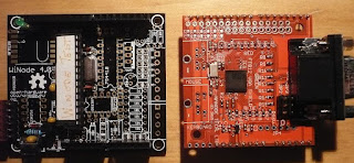
During testing, I also made good use of an old ATmega328 board I designed a few years back - the WiNode.  It's an uncluttered Arduino "clone" that works at 3V3. I use these for quite a few small projects - as I have about 50 remaining in stock from an earlier project. They are in the form of a through hole kit - and can easily be soldered up in about half an hour.

The WiNode pcb can provide just the basics - a minimal 3V3 Arduino with access to the headers. This board will execute the GameDuino2 Library - with minimal modifications - and has the benefit of  a uSDcard holder on the underside of the board. There is also a battery backed RTC, 32Kx8 SRAM and an H-bridge that can be used as a class D digital amplifier for driving small speakers.  Adding video to such a useful board with further increase its application.


WiNode and SVGA Shield together for comparison
Conclusions

The SVGA shield concept works and is capable of producing an 800x600 SVGA video output for a monitor - using an IC that was really intended for compact LCD modules.

The hardware was simple and straightforward - the biggest problem was reliably soldering all the pads of the 56 pin QFN package.

The board can also accept a PS2 keyboard and mouse - and a welcome addition on a future version would be a microSDcard socket - allowing images to be down loaded from card.

The board works with a very basic 3.3V  SPI interface up to 30MHz  spi-clock - requiring just 5 signals - plus 3V3 and 0V.  It can be added to any microcontroller that presents the original Arduino expansion header pattern, with the SPI bus available on D11,D12, D13.

Some hours later - I could do this.....


Making a new product in a month - An Engineers Life in 140 Characters or Less

$
0
0
A new product always starts with an idea.

In late November, I had been reading about various ways of producing a low cost VGA video output from a microcontroller.  Having dabbled with VGA on the ZPUino soft core processor on the Papilio Duo from Gadget Factory, I realised that if any small microcontroller could be assisted to produce stunning video effects and support a sophisticated user interface at minimal cost - then it would be a major innovative step.

I read about the new EVE (Embedded Video Engine) ICs from FTDI in Glasgow and ordered a dev-kit in early December. At the same time I started work on a board layout for a new minimalist VGA shield.

1st Draught - Will it all Fit?
I had been musing throughout the Autumn about a new board format of just 50mm x 50mm  - in order to make full use of the special offers from the low cost Chinese board houses - so my first attempt was to see if I could even get the VGA and PS/2 connectors onto the standard board template. Above is my efforts - dated November 26th.

Over the 1st weekend of December (5th, 6th) my ideas blossomed, and grew - and so by the end of the the first week of December I had a 56 pin QFN package footprint worked out plus something that approximated to a FTDI EVE chip on a board. With the basics in place - it was just a case of finishing the layout and tidying up.

Main FT812 IC partly routed

By the 9th of December - the design was nearly ready for sending off - and this was further reinforced by a message from my board-house saying that pcb designs sent in before the midnight on the 10th of December would be delivered before Christmas - and with a 10% discount.

Almost ready for prototype production
On December the 10th - a very busy day to get 2 new designs delivered to @Ragworm by midnight. This tweet hints at the urgency that Thursday

So the pcbs went off to Ragworm on the night of 10th December, and then we were in for a bit of a wait, until they were delivered before Christmas. Also on the evening of the 10th, I forwarded the EagleCAD files to my friend James Bowman (@GameDuino) who lives near San Francisco - so that he could have a go at having a duplicate set of pcbs made - independently of mine.

In the mean time I got on with another pcb design - this time for a low energy Bluetooth device - and spent 3 wonderful days up in North Wales at #BothyHack3 - where I designed some, yet more pcbs.

On the 22nd of December, I received a package containing the prototype boards - I tried a bare board for size on one of the FPGA platforms we were considering:


So that evening I built up the first prototype:


Christmas activities then got in the way for a few days - but on the 24th James reported that his pcbs had just been delivered in California from China - having been held up for over 24 hours in Fremont, California:


So with Christmas almost upon us - Festivities kind of impeded progress - also known as a well deserved rest. I have done 20 unique board designs in the last 24 months......
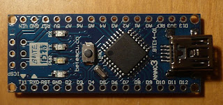
So on the Morning of 28th December, I crawled out of the post Christmas hangover haze and thought about exercising the new VGA hardware.  It took longer than I thought - but by 1am, and a couple of false starts - the VGA hardware sprung into life and created its first image.


From large red blobs served in the early hours of the morning I progressed to a simple text display:


But then on Tuesday evening - James came back with the stunning tweet that he had pushed the resolution up to 1024 x 768  60Hz. So at that point I suggested that I get my coat.....


I hope you have enjoyed this light-hearted look at how modern engineers collaborate across global frontiers and timezones - using social media to full advantage - in order to expediate the development of a new fun product.  From concept to first prototype executing code and exceding all expectations in just a month.  Shouldn't we all be working smarter, not harder?

And remember - when it's 2am in Britain - it's only "Beer o'clock" in Northern California!

Thanks to all my friends and colleagues in Kent, Sussex, Denver and Northern California who have helped make this happen so quickly.


Happy New Year - and all the best for 2016!


New Year's EVE & EVITA

$
0
0
Last Post of 2015.

Tonight, a bit later, I will be celebrating the New Year, but for the next few hours I am working hard on a new 50x50 pcb design - more on this later.

This week, as readers might know,  I have been involved in a Trans-Atlantic collaboration to develop a new prototype board for an Embedded Video Engine or EVE chip - manufactured by Glaswegian firm FTDI.

In a hectic week, a team working in the UK and also in Northern California - have got the hardware running - and are now able to produce a big bright graphics display on a large screen monitor - using virtually any "Arduino -like" microcontroller development board.  For only a few dollars - you can now add high quality 24 bit video and audio to your latest project - and there is not a Rapberry Pi in sight.

Here's an example of what James and Felix (pictured) achieved in California on Tuesday.
Felix solders whilst James writes code...
Meanwhile in the UK I was successfully creating an image of a big red blob....


The EVE chip is normally used to produce a video interface for LCD touchscreens - but with a bit of tweaking and a few precision value resistors we have got it producing reasonable quality 24-bit RGB video for displaying on monitors or TVs that have the usual VGA (15way Sub D) connector.

This allows virtually any small microcontroller to produce good quality graphics - and in the case of the prototype - any board that supports the Arduino expansion headers.

With a few clever tweaks to the timing, James in California has succeeded in obtaining a 1024 x 768 60Hz resolution - sometimes known as XGA.  This exceeds the published specification of the chip, only by a small margin - but as James is expert on these matters, he assures me that there is no cause for concern.

Just in Time for the Party - Meet EVITA

Whilst the prototype was a quick design just to prove things are working - and so far they have exceeded all expectations, I am currently working on an upgraded  new board, that is most likely to be a commercial product.


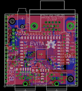
The EVITA board uses the same FT812 EVE chip, but adds a microSD card socket, audio output from a 3.5mm jack and unlike the prototype is now 5V tolerant - so you will be able to use this on a 5V Arduino - without "Fear of Frying".  EVITA offers a better overall layout, more signals are available for the experimenter, and better still, it is compatible with GameDuino 2.

If you add EVITA to a humble Arduino, you have essentially the basis of a full computer system, with connectors for Keyboard, Mouse, Audio and glorious XGA video output.

Right from the start, EVITA is open source hardware and open soft software.  If you are good at fine, surface mount soldering, you could purchase a bare board cheaply, stock up on the components and build your own in a couple of hours. All of the information is available online, including datasheets, code libraries and a vibrant community forum.

In the next few weeks there will be some more pcbs released in the 50x50 format.  These will allow you to add a custom ARM processor to EVITA and make up exciting new projects.

More of this in 2016


Ken


Meet Evita!

$
0
0
EVITA - Almost ready for PCB Manufacture
On New Year's Eve, I posted a little about a new board which I am designing.  The CAD files are almost ready for production - so this little EVITA board is going to be the first new design of the year.

EVITA uses the next generation of EVE IC from FTDI  - in this case the FT812 or FT813. Instead of outputting digital video data to a TFT LCD module, EVITA uses a set of resistor networks - actiing as digital to analogue converters, to allow the analogue RGB signal to be reconstructed. In this way, EVITA can display full 24 bit colour on a large screen monitor or TV up to a resolution of 1024 x 768 pixels at 60Hz - provided that it has a VGA connector.

EVITA is fundamentally a graphics co-processor, built onto an "Arduino" shield.  With the standard Arduino expansion headers - EVITA will fit a wide range of microcontroller and FPGA development boards - from a variety of different manufacturers and IC vendors. EVITA has been designed to be a universal graphics adaptor - for small microcontroller projects.

EVITA adds bold, high resolution graphics, images and MPEG movies to your microcontroller application.

Use it as a versatile video interface for retro-gaming,  as a complete computing shield for retro-computing with keyboard, mouse and audio interfaces or as a stunning  video enhancement to your latest Arduino project.  Develop complex graphical user interfaces on the big screen - before porting them to a LCD module.

Here are some of the main features:


  • XGA Video Output   1024 x 768 pixels at 60Hz  24 bit colour
  • Capable of high resolution animated graphics, JPG viewing and MPEG Playing  
  • Arduino shield footprint - to suit most dev-boards
  • 5V tolerant inputs.
  • On chip audio synthesiser with 3.5mm jack Audio Output
  • Micro SD card holder for storing graphics, JPG and MPEG video
  • PS/2 Keyboard Interface
  • PS/2 Mouse Interface
  • Low cost Open Source Hardware and Software
  • Pin Compatible with GameDuino 2
  • Suits any microcontroller or FPGA  - Arduino/ZPUino GameDuino 2 library available
  • Low power - can be used in battery powered applications.

EVITA has been developed in collaboration with James Bowman at Excamera Labs and Jack Gassett at the Gadget Factory.

We hope to have samples of EVITA available through the Gadget Factory for the early spring.

James has put together a timely video demo:

Happy New Year.


Colour Coding - Part VI

$
0
0
"Coming Up For Air"

The last week whilst not at work, has been a bit hectic.  I have managed to get video output from the first prototype FT812 board, and completed a new pcb layout for the pre-production prototype - which is now called EVITA - a low cost XGA graphics adaptor.

The pcb artwork for EVITA has been sent for manufacture


EVITA has a number of attractive new features - not present on the earlier prototype:


  • 1024 x 768 60Hz XGA Graphics
  • micro SD card for storing images and videos
  • Audio synthesiser and output via 3.5mm jack connector
  • 5V tolerant - will now work with 5V Arduino - without risk of damage
  • Faster data transfer using QSPI  (Quad SPI)
  • Hardware pinouts compatible with GameDuino 2
  • Works with a multitude of different microcontroller and FPGA development boards. 

EVITA provides a complete video, audio, keyboard and mouse subsystem for any retro-game or retro computing project.  It is compatible with Papilio Duo, Nucleo, Discovery F7, Arty, and many of the Arduino like dev-boards.

Meanwhile, James Bowman, in Northern California reported on December 29th that he had achieved XGA resolution of 1024 x 768  60Hz - which is something of a game-changer. The XGA shield was fitted to a Papillio Duo FPGA board running an instance of James's own J1b Forth processor. This increased resolution opens up a whole lot more applications.

In this post, I pause for thought, before diving into the next part of the FT812 XGA Shield development. I consider potential applications - now that we have a universal video board that can be added to a wide variety of microcontrollers - both big and small.


The EVE (embedded video engines) work on the principle of a "Display List" of objects that the microcontroler sends to the FT8xx as a series of SPI commands and data.  The list of objects can be generated "on the fly" by the microcontroller - so as to provide an interactive user interface, such as an animated game - in which the motion of the characters is controlled on influenced by the User input. Alternatively the display list can exist as a "pre-canned" static display, stored in memory, - either flash or RAM, or communicated to the mcu via some communications link.

It's this latter option that I believe will open up a range of applications.

Compressing the Bandwidth

We are all familiar with how a browser application can create a web page from a few lines of HTML, and that the raw HTML code may easily be transferred via a communications channel - such as ethernet, WiFi or 4G.  The HTML is effectively a form of shorthand - and it is the job of the browser to convert this code into a graphic-rich web page.

In a similar way, the display list commands for the FT8xx could be conveyed over a relatively low bandwidth link - such as serial, ethernet or low power wireless - and then the FT8xx renders this fairly compact display list into an attractive graphical user display.  However, a typical display list could be 10,000 characters long, and sending such a list might lead to complications with very low bandwidth communications channels.  This is where I believe the idea of "pre-canned" screens may be applicable.

The Universal Instrument

Suppose for example, you are an electronic engineer, and you really only want to carry around one bit of equipment  - like a multimeter or handheld 'scope.  By "pre-canning" the user interfaces for a range of instruments such as DVM, 'scope, logic analyser, chart recorder/datalogger, decibel meter, thermometer, infra red flir imager - then all of these instrument "identities" could be stored in flash - and you could easily switch between them.

So in theory, the only information that would need to be sent to the "Universal Instrument" would be a value, an a tag that described it's identity, and what UI screen to display it on - a datagram.

Big Screen Beckons...

Furthermore - if the data to display can be greater condensed - it can be conveyed via a low bandwidth link - for example BLE.  Then the XGApcb  may be packaged as a "dongle" that is plugged into the back of the TV or monitor via the VGA port - and all the data conveyed from the instrument to the large screen via BLE.  Equally so, a handheld device such as a smartphone or tablet, could run an application that generates the UI datagrams.

As the XGA shield has shown - the FT812 is just as capable of generating an image for a large screen monitor as it is a compact LCD.  If the image format was correctly chosen - it might even be possible to have a large monitor display a duplicate of the image on the LCD. This opens up the possibility for small portable instruments that can also display on the big screen - like a scope or logic analyser with a 32" screen for example.

Whilst this will never replace some of the existing plug-in devices - such as Chromecast Amazon FireStick, or some of the linux SBCs like Raspberry Pi or "Chip" - for some applications it may be convenient where 1024x768 graphics is more than adequate.

Some New Features

The Evita design is currently undergoing some updates - such that it will contain additional hardware - for even more useful features:


  • Interface to a Wii Nunchuck controller - for accelerometer, joystick and button controls.
  • Allow a LCD of up to 7" and 800 x 480 to be driven as well as the external big screen monitor
  • Interface with FPGA hardware to allow a HDMI video interface to be used.
  • Extensive graphics library in both C and Forth.

We have probably reached the point where a 7" tablet would make a great user interface for the Universal Instrument - costing about  $50.  Is there really any point building anything for yourself these days?

The Learning Machine.

Of course there is a point to doing things for yourself - it's called education.

I would probably have no idea how to plot a pixel or draw a line on the screen of a PC or a tablet - it would involve someone else's application code, that I know little or nothing about, nor the way in which the operating system drives the graphics processor.   For the newcomer or student of Computing Science, there is a huge amount of historical information to take on board, before these modern systems can be properly understood.

With Evita - coupled up to a fairly modest microcontroller - a few simple commands can produce colourful animated graphics.  If you want to know more  - it's all in James Bowman's Gameduino 2 Book.

Being able to output colourful text and graphics with a few commands, really increases the interaction potential between user and computer. It also brings back the joy of learning programming, immersed in a colourful world where a few keystrokes can create stunning graphical effects.

I have mentioned in previous posts the "Nand to Tetris" course - which takes the computing science student through the whole process of designing a modern computer system - hardware plus all the layers of software  starting essentially with Nand gates.

When the "N2T" course started in 2005, FPGA hardware was not widely available outside industry or academia, and 7" colour LCD touchscreens were a bit more than $50.  Now that there is a lot of cheap hardware available, it would seem sensible to revisit the N2T course and add in a substantial hardware element - based on modern low cost hardware.

A low cost FPGA board  (about $50 to $100) and a video subsystem consisting of a 7" LCD touchscreen and the EVE embedded video engine would allow a wide range of hardware oriented teaching modules to be taught.  For about $200, a first year student could design and build a complete, portable embedded computer - capable of running a high level language, using a soft core processor running on a FPGA - designed from scratch.

The handheld computer could be used for datalogging, controlling lab experiments, instrumentation and measurement (DVM, oscilloscope etc), note taking, game playing and a myriad of useful tasks. Students would become intimately familiar with the inner workings, during the course of their studies, that they could produce hardware add-ons, and share these designs with other students - worldwide.

I hope to cover this topic in greater detail in a later post.


Meet Fobble - a general purpose Wireless Breakout Board!

$
0
0
Fobble - A General Purpose Wireless Breakout Board

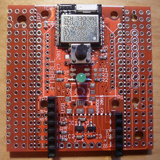
This week I have been working on another of my standard footprint 50mm x 50mm boards - it is a general purpose wireless module carrier board:-  Fobble.  That's a BLE Fob - for anyone who misses the pun.

In the last few weeks there have been a number of applications arise - that could easily be addressed with an easy to use, generic wireless platform. These have included keyfob or pendant applications - requiring a small coin cell powered board - to a generic wireless board that can be stacked to one of the processor boards to provide wireless connectivity.

So after a week of head-scratching, I have come up with a small board, which at least meets the requirements of the development phase of the project - once again a useful, flexible dev-board that hobbyists can experiment with.

As can be seen from the above picture it contains a number of key features:


  1. A resident RFduino  Bluetooth Low Energy Module with ARM Cortex M0 processor
  2. 2 layer pcb 50 x 50 mm format- with extended Arduino headers pin-out
  3. An X-Bee footprint - with 0.1" breakout headers - to add your own wireless module
  4. Two push button switches - only 1 populated shown
  5. Footprint for RGB 0505 LED
  6. Detachable power and programmer section
  7. Detachable side panels - to make 38 x 32 mm BLE Key Fob 
  8. 8 pin header to accept 1.3" OLED display
  9. 20mm coin cell or flat Li Po cell power - on rear of Fob pcb
  10. Micro - USB connector for recharging Li Po
  11. Side Prototyping areas - perforated in 0.1" matrix
  12. 7 pin and 5 pin headers to accept any RFduino accessory shields - for development work

Some applications include:
  • A low power wireless data display using BLE and either OLED or e-ink display.
  • A BLE key fob, or wearable pendant with 2 user buttons and an RGB LED
  • A bridge between BLE and low power 433Hz or WiFi
  • As a wireless shield for an Arduino compatible device
  • As a general purpose Experimenter's BLE dev-board.
The other unique feature about Fobble, is that it has it's own native ARM M0 and Bluetooth Low Energy module, and can act as a bridge between Bluetooth, and any other wireless module that you may wish to use.

It can accept any wireless module that offers an XBee footprint - or a wireless daughter module of your own making - pinned out to 2,  10 pin headers  on 1.1" centres.  This simple scheme offers the most flexibility. So you can add an ESP8266 on an X-Bee format carrier, or similarly an RFM69.

Fobble is pin compatible with the standard Arduino header footprint, and will also accept a 3.3V FTDI cable for programming.

Small & Versatile


With side-wings removed Fobble becomes a compact 32 x 50 pcb


As can be seen from the above layout plot and the vertical parallel white lines, the centre section of Fobble is perforated with a line of holes - so that the outer wings that carry the Arduino headers may be snapped off. Additionally the bottom section that has external power supply components may also be broken off to leave a 32 x 38 mm section that can be mounted in a small key fob style case.

Another feature of Fobble is that you can  plug in a low cost OLED graphic display - and create a Bluetooth message display.  The display chosen is the Adafruit 1.3" diagonal OLED display but other similar displays may be used with minimum changes to the wiring.

The availabilty of pluggable headers, plus the uncommitted Arduino pin headers mean that Fobble may be used to prototype new wireless ideas - just by using jumper wires, or a breadboard.

The onboard module is the RFduino - based on an ARM M0 processor - the Nordic Semiconductor nRF51822.  This is programmable via the Arduino IDE and can make use of the Adafruit OLED graphics libraries.

Expandable

Fobble recreates the standard 7pin - 5pin header pattern used by the RFduino Ecosystem - thus allowing any of the existing modules to be plugged in - including the USB programmer - or you can just use a serial programming cable that has RTS for resetting the board - such as FTDI cable or CP2102 adaptor board. A wide variety of prototyping modules are available in this format - produced by RFDigital - and distributed by RS, Mouser, Digikey etc.

Fobble can be used with these open source Arduino communication boards.

PCB Layout


Fobble - the latest 50x50 format board for Wireless Breakout 

Here's a shot of the layout of the 50x50 pcb - showing the white lines where the board is perforated to allow the side wings and the lower power-supply programmer section to be snapped off.  The 2032 coincell is mounted centrally on the underside of the Fob section.


Stop Press!

The company behind the RFduino have just announced a new BLE module called Simblee
It shares the same development module as RFduino - and now available from Digikey and Mouser - Exciting times ahead!

A Versatile 8 bit Computing Platform

$
0
0
Part Populated WiNode Board
Back in late 2011, I designed a product called WiNode, which was a companion product to the Nanode RF - a simple Arduino based wireless to ethernet hub.

Well that's all ancient history now - but I do still have a box of 40 WiNode kits left over - which I am slowly finding uses for.

WiNode was conceived as a jack of all trades.  It had the usual 16MHz ATmega328P processor - but in addition a whole lot of hardware goodies.

  • 32K SRAM with super capacitor back-up
  • microSD connector
  • RFM12 Low Power 433MHz Wireless transceiver module
  • MCP79410 Real Time Clock - again with supercapacitor backup
  • 754410 Dual H-Bridge (for motor, stepper, relay driving - or Class D audio Amplifier)
Despite all of the additional hardware, WiNode was a compact but surprisingly uncluttered layout. Almost all of the components were through-hole  - so easy to solder.  It was the perfect platform for a whole lot of Arduino & Low Power Wireless control an monitoring applications.

Now 4 years later - WiNode is going to get a new lease of life.

With the SD card, Realtime clock and additional 32K x 8 RAM it makes an ideal platform to host some of my 50x50 series of shields including the new Evita High-Res Video Shield.

Using the Gameduino 2 Library - the hardware is virtually identical to the Gameduino 2 - except that the Evita board drives an external display - in this case below a 32" wide screen TV

Black Text 128 Characters per Line 1024 x 768 


A very large clock in just 14 lines of code
Whilst the applications above are very simple - and easy to code using the comprehensive Gameduino 2 library, there is sufficient capability in the 8 bit ATmega to produce a retro-computer - not unlike those used in the mid 1980s. 

The Evita shield also offers  PS/2 Keyboard and Mouse connectors, and audio output - allowing a complete 8 bit computer with high resolution video to be created.

Additionally it is easy to add a Wii Nunchuck to the I2C pins - making it ideal for playing games or retro computing. The Nunchuck derives its power from the two unused pins A2 and A3 set LOW and HIGH respectively.

With the right language - such as Tiny Basic or Forth, it could make a very versatile computing platform - and ideal to teach basic programming techniques.

The TinyBasic code gan be found here on Github

Hardware Allocation

D0          UART RX
D1          UART TX
D2          FT812 INT
D3          KBD_CLK
D4          KBD_DATA
D5
D6          MOUSE_CLK
D7          MOUSE_DATA

D8
D9          FT812   /CS
D10        FT812  PowerDown/Reset
D11        SPI MOSI
D12        SPI MISO
D12        SPI SCK
D14        I2C SDA
D15        I2C SCK

A0          Analogue Joystick (X)
A1          Analogue Joystick (Y)
A2          Wii Ground
A3          Wii Power
A4          Wii Nunchuck SDA
A5          Wii Nunchuck SCL


Details of interfacing the Wii Nunchuck may be found here.


More Thoughts on Retro Computing

$
0
0
Forty years ago when home computers were in their infancy - and I myself was still in short trousers, the tech community in Silicon Valley began to build their own homebrew computers based on the newly available microprocessors such as the 8080, 6800 and 6502.

Microprocessors were still expensive (especially Intel) but with the advent of the considerably cheaper 6502 in 1975 there was a significant reduction in the overall cost of a homebuilt machine. The Homebrew Computer Club - that met regularly at Stanford University soon obtained a copy of a cut down interpreted programming language called Tiny Basic, and very quickly it was being adapted to run on all sorts of fledgling machines - a process that involved a lot of tedious copying of listings,  saving onto paper tape or cassette, or even programming onto Eprom.

The early pioneers desperately wanted an easy to use language, in plain English text that was quick to learn and quick to program.  They put up with perhaps limited maths capabilities and lacking in anything but single alpha-character variables,  but the advantages more than overcame the shortcomings an so it was Tiny Basic that helped seed the early microcomputer industry.

Wikipedia has a good account of those early days of TinyBASIC.

Tiny BASIC was compact and designed to fit into about 2 - 3 kbytes of memory - as the early micros generally only had between 4K and 8K of memory - similar to what the first minicomputers had, - a decade earlier.

In some implementations, it was coded in such a way that it would run within a virtual machine on the microprocessor.  This approach led for compact, more portable code - but was not so fast in execution as an implementation coded in the host's native machine language.

1970s

In the mid-1970s microprocessors could at best muster about 1 million instructions per second - but still were able to deliver a credible computing experience when programmed in TinyBASIC.  The first machines generally used teletype or serial terminal for input and output - the ASR33 Teletype being favoured - as it had built in punched paper tape reader and punch which conveniently provided a permanent paper tape record of the program - which could be swapped and exchanged amongst friends at the computer club meetings. When I went through university in the early 1980s - the engineering department were still using 20 year old ASR33 Teletypes!

1980s

Within a few years, the large corporations became interested in the home computer market - and the products were further refined to be more home-friendly.  This involved incorporating some video generation hardware into the design - so that the output could be displayed on the home TV.

Whilst this increased the market appeal, it meant that often the poor overworked microprocessor was further burdened by the overheads of servicing the video display - and that real processing was constrained to the vertical blanking interval - slowing the machines down further.  Early Sinclair machines (ZX80, ZX81) had been honed down to the bare minimum hardware, in order to undercut the cost of competitor's machines - and so the resulting operation of running basic was particularly slow.

Recent benchmarking tests show that a 3.5MHz Z80A - as used in the Spectrum was capable of about 0.142 DMIPS.  Or 250.7 Dhrystones per second.

1990s.

Microprocessor clock speeds increased rapidly over this decade.  The very popular Atmel AVR appeared in 1996 and was capable of being clocked at speeds of up to 20MHz.  The modified Harvard architecture featured a 2 stage pipeline, allowing execution of one instruction whilst the next is being fetched. This gave operational speeds of approaching 1MIP per MHz - so a 20MHz processor would achieve about 20MIPS.

The AVR was optimised for executing high level languages - especially C, and as such has a highly orthogonal instruction set.

There have in recent years been several implementations of Tiny Basic, written in C and aimed at supporting, in particular, the Arduino or Arduino derivatives. The code often supports external accessories such as a micro SDcard used as a disc, external SRAM and on chip EEprom  as well as the usual Arduinio I/O  and timing - such as millis and micros.

The code is reasonably fast allowing an AVR (16MHz)  to execute about 50,000  empty For-Next loops per second. (This was implemented on an Arduino back in 2011 - see my earlier post from May 2011.

The New Millenium.

If we now fast-forward a few decades, we now have multi-core 32 bit processors capable of executing a billion instructions per second, on each core - and handling larger numbers and larger data sizes.

How would TinyBasic perform on a modern ARM processor for example? Would the interactive nature of the language, easy to learn syntax and the additional resources - memory and peripherals offered by a modern ARM processor make for a rewarding computing experience?

As there are versions of Tiny Basic written in C, it should be fairly easy to port it across to almost any microcontroller. Right?

Benchmarks and Other Performance Indicators

Recently I have been looking at the benchmarks of various ARM processors - especially those that are compatible with the Arduino IDE.

These include the STM32F103 and GD32F103 running at 72MHz and 120MHz respectively. (The GD32F103 is a Chinese produced, licenced version of the STM32F103 - tweaked with faster on chip RAM so it runs at 120MHz).  These may be programmed using the  STM32duino plug-in within the Arduino IDE.

Peak Performance

A very wide range of processors may be programmed within the mbed ecosystem - including the latest Cortex M7 from ST Microelectronics.

The STM32F746  is a Cortex M7 with 1Mbyte of Flash and 384KB of SRAM.  Available in a number of LQFP packages from 100 pins to 208 pins, it is clocked at 216 MHz and claims to deliver 462 DMIPS.  Here's the spec summary:


  • 1MB of flash memory and 340KB of SRAM (320KB system, 16KB instruction and 4KB backup SRAM)
  • Ethernet, 6/3 SPI/I2S, 4 I2C, 4/4 USART/UART, USB OTG FS/HS, 2 CAN, 2 SAI, SPDIFRX, SDMMC interfaces
  • 168 I/O ports with interrupt capability
  • 8bit to 14bit parallel camera interface up to 54Mbytes/s
  • Ten general purpose, two advanced control, two basic and one low power timers
  • LCD-TFT controller up to XGA resolution with dedicated Chrom-ART accelerator for DMA2D
  • Three 12bit, 2.4MSPS ADC with 24 channels and 7.2MSPS in triple interleaved mode
  • Two 12bit D/A converters and 16 stream DMA controller with FIFOs and burst support

  • This looks an impressive spec for a device that costs about £11 in 1 off.

    The STM32F746 is about the fastest processor I can lay my hands on, and being LQFP, solder onto a pcb.  Using the online mbed compiler it can be programmed without having to resort to expensive toolchains.

    The STM32F746 forms the basis of the STM32F7 Discovery board - a $50 development board with LCD, USB, ethernet, microSD card, SRAM, and a whole host of other features.


    • STM32F746NGH6 microcontroller with 1MB flash memory and 340kB RAM in BGA216 package
    • On-board ST-LINK/V2-1 supporting USB reenumeration capability
    • USB functions - Virtual COM port, mass storage, debug port
    • 4.3" 480 x 272 colour LCD-TFT with capacitive touch screen
    • Camera connector
    • SAI audio codec
    • Audio line-in and line-out jack
    • Stereo speaker outputs
    • Two ST MEMS microphones
    • SPDIF RCA input connector
    • Two pushbuttons (user and reset)
    • 128Mb Quad-SPI Flash memory
    • 128Mb SDRAM (64Mb accessible)
    • Connector for microSD card
    • RF-EEPROM daughterboard connector
    • USB OTG HS with micro-AB connectors
    • USB OTG FS with micro-AB connectors
    • Ethernet connector compliant with IEEE-802.3-2002

    If we then make use of an embedded video engine  - or EVE chip, to drive a graphics display we could potentially have an ARM based computer with full colour high resolution graphics that runs about 1000 times faster than the ones we remember from the 1980s - and for a cost of about £20.

    My prototype EVE board is designed to plug into the underside of the STM32F7 Discovery board and provide full 1024 x 768 video output and a PS2 keyboard and mouse interface.   This combination would make a very comprehensive computing environment.

    In my tests I achieved about 300,000 Dhrystones per second  - about 1200 times the speed of the old Z80.


    A Review of Tiny Languages Part 1

    $
    0
    0
    Tiny Languages

    This week I have been looking at bygone computers and some of the languages they used - tailored to work within the framework of their resource limited hardware.

    My recent dealings with the "Forth-like" SIMPL language has led me to look for other examples of minimalist programming languages.  Many of these were devised in the 1970s and 1980s - when home microcomputers were very short of memory resources.

    In this post I look at some very small computer languages - often less than 4Kbytes in size.

    My recent search has unearthed the following:

    VTL     Very Tiny Language   - a BASIC like language for resource limited microcontrollers

    VTL-2   An updated VTL with more features -  yet assembles in 768 bytes

    Mouse  - developed in the late 1970s for electronic music applications on a PDP8

    TinyForth - A cut down Forth, written in C or assembler

    Txtzyme - an I/O oriented minimal control script with some Forth-like features

    SIMPL     - an extended version of Txtzyme to run on several platforms.

    TinyBasic  - various offerings available. TinyBasicPlus

    Bitlash  - a control oriented, Programmable Command Shell to run on Arduino


    VTL

    VTL is an interpreter designed in 1977 by Frank McCoy for the 6800 and 8080 machines of that era. The complete 6800 version of his interpreter is ROMable, IN 768 BYTES!

    VTL was originally devised for the Altair 680 - an early 6800 microcomputer, with a strong similarity to it's stablemate the MITS Altair 8800 but much smaller in size.  It had 1K of RAM and sockets to accept 1K of ROM.  ROM chips at this time were likely to be only 256 bytes - so 4 sockets required!

    There appears to be a following for VTL and its derivatives in Japan - so many of the references are Japanese websites - but easily translates with Google Translate.

    Summary of VTL languages over the years - translate from Japanese

    "Creating a VTL Language" Some description of VTL for 6800, 8080/Z80 and AVR  - source code in assembler and C - Translate from Japanese. This site and source code provided by T. Nakagawa.

    The author, T. Nakagawa, has provided source code (about 370 lines - see this Github Gist) that will run on an Arduino with a bit of fiddling. You will need to add the serial putchr and getchr routines to drive the UAR - and include the UART code from AVR-Lib.

    Once these are added, it compiles to about 2.6K under the Arduino IDE.  It should be noted that the AVR uses a 16 bit instruction word - so the byte count for AVR Flash code is generally about twice that of other 8 bit microcontrollers.

    If you want to try out VTL - this is a packaged exe that runs on a PC in a command prompt window.

    VTL remains of interest because it has some very compact C code for the various building blocks of a simple interpreter - and is relatively easy to understand its operation.

    VTL-2

    In 2007, some thirty years after his original VTL offering, Frank McCoy revisited his VTL and produced an extended and improved version of VTL - which still fits into 768 bytes (on 6800)   The User Manual and some example programs are here.

    Mouse 

    Mouse is a very small language that was written in the late 1970s - early 1980s by Peter Grogono.

    It was a further development of his early 1970s system/language MUSYS - that was written to aid his work with early computer generated electronic music on resource limited PDP-8 machines.

    Mouse took aspects of MUSYS and updated them to suit the late 1970s emerging microprocessor scene.

    Here are some links:

    The Mouse Programming Language

    The Great Mouse Programming Language Revival

    Wikipedia has further links that may be of interest.


    Tiny Forth

    This site and source code is again provided by T. Nakagawa, a Japanese enthusiast of Tiny languages.

    He has written TinyForth both in well commented AVR assembly language (1964 bytes) and also in C that closely follows the assembly language. This not only gives a good illustration of how the language has been constructed but also how closely AVR assembly is matched to C.

    I have created a Github Gist for this TinyForth - complete with UART getchr and putchr routines. The code compiles to 4854 bytes - I used Arduino 1.04  IDE - as I had some difficulty with later versions with getting the UART code to compile.

    It appears to be a subset of Forth - but with sufficient keywords currently available to do simple tasks  - but like any Forth is easily extended.

    Input and Output is via a serial UART interface only - it would need further extensions to the dictionary to build up a vocabulary of I/O and timing functions for the Arduino/AVR.

    The AVR assembly language version is much more compact - I have added a fully commented version to this Github Gist 

    If you want to write a Tiny Forth for an AVR or even an ARM - then this is a good place to study the basic language structure.

    In conclusion - TinyForth looks like it could provide a useful kernel for a larger project. It would be worth compiling this source for an ATmega1284 - the extra RAM (16K) and additional I/O port would make a very capable Forth Computer.

    As a newcomer to AVR assembly (but having done a lot of Z80 years ago) it is rewarding to see how readily C code can be translated to assembly language.  A lot of the Forth primitive wordss are of immediate use for the Txtzyme/SIMPL interpreter (see below) - and having the C and assembler code together is a useful crib on how one might take the project forwards further.


    Txtzyme

    Txtzyme was created around 2010-2012 by Ward Cunningham.  Txtzyme has the advantage that it is specifically oriented to I/O control and interaction - yet surprisingly simple.

    The Arduino version allows simple control of the Arduino I/O and allows timing functions and loops. LED sequences, musical tone generation and printing serial output of analogue sensors are easily performed.

    It is simple in nature - essentially just a single character  interpreter contained within a loop. It uses a single stack variable x to control some parameter of the operation. It is fairly simple to understand and easily extendable to include further "words" such as arithmetical and logical functions.

    The Arduino version is just 90 lines of code and compiles to 3518 bytes. The codesize can be much reduced by replacing some of the Arduino C functions with more compact code, possibly even resorting to AVR assembly language in order to make a more compact kernel.

    The beauty of Txtzyme is it's simplicity and the fact that it can be easily tailored to suit a particular application.

    Reducing the Code Size:

    Removal and replacement of the Arduino Serial code and using a custom function to print a long number can bring this down to 1884 bytes.

    Removal of the Setup() and loop() functions and replacing with a main() and a while(1) will reduce it to 1782 bytes - but at a loss of the timing delays and millis() functions

    Removal and replacement of the Arduino delay and delay_microseconds code will bring it down to
    1484 bytes.

    Replacing digitalWrite with a simplified function  - reduces it to 1040 bytes

    Removal of analogRead and digitalRead  reduces it by a further 92 bytes to 948 bytes.

    digitalRead alone is 272 bytes!

    If you want to try a cut down version of Txtzyme - I have paired out most of the bloat and put a 658 byte minimum kernel here.  It doesn't do much - you have to add your own functionality in the form of case statements.

    Txtzyme appears to indicate that a I/O oriented micro language is possible on the AVR (Arduino) in about 1024 bytes. This makes it  possible to include it with a bootloader plus some extensions in under 2K.

    The code-shrunk version of Txtzyme is available on this Github Gist   You may wish to re-instate digitalRead  (line 110) and analogRead (line 150) depending on your requirements.


    Next Time

    In the next post I look at SIMPL and how it has evolved from Txtzyme.


    A Simple Computing Platform

    $
    0
    0
    Is this how modern computers appear to users - even experts? 

    It is becoming ever increasingly clear to me - and others, that computing platforms have become just too complex. In an attempt to be all things to all users they are built on a massive agglomerate of software, some which has it's roots in the 1960s, and most people have forgotten why it was there in the first place. Literally they have become a tower of Babel

    Reading the Wikipedia entry - the Tower of  Babel was a huge edifice - so big that no-one really knew how big it was. Ironically it was created, so that everyone living in Babel could speak the same language.  According to the myth, the big chap upstairs didn't like this, and confounded the people's speech, so they could no longer understand each other. He then destroyed the tower and sent it's residents scattering to the four corners of the world, and this led to the diversification of language.

    Loosely applying this myth - as an analogy of the current state of the computing industry - we are now trying to recreate a Tower of Babel, as a concretion or conglomeration of thousands of different software elements, loosely tied together in a Linux wrapper - in the hope that they somehow will fuse to form a unified entity.

    Well just as Babel ultimately failed, I believe that our current strategy of building  vast megalithic operating systems - then spending all our time worshiping them, is a road to ruin.

    Like I might say to a historical resident of Easter Island "Keep on carving the stone heads, Dude,  - just wait and see exactly where that gets you!".

    If you, like me, are fed up dealing with gigabytes of someone else's software in multiple non-compatible languages then this recent article from "The Register" may be of interest.

    Project Oberon

    This was an ambitious project started in 1985 to create a simple workstation with it's own lightweight language and operating system based on Pascal / Modula 2.  The chief designer was Niklaus Wirth - who also was lead designer with Pacal, Modula 2 and other languages.

    Fast forwarding to 2013, Project Oberon has been recreated in the form of a low cost "OberonStation" using an inexpensive Xilinx Spartan 6 FPGA - accomplished by Paul Reed and Victor Yurkovsky - a regular FPGA Blogger.

    The Oberon Station - Spartan 6 FPGA plus 256Kx32bit SRAMS

    If you wish to look further at Project Oberon - a pdf of the 2013 Book is available - with html index here.

    Thoughts- and Questions on OberonStation

    Less is more - this hones down a workstation to the level of complexity where any one can understand the hardware.  It is reminiscent of Chuck Moore/Jeff Fox's Ultratechnology Workstation in a mouse

    The Oberon Station boots from the uSD in about a second - which is impressive. My laptop thinks for about 5 seconds before it even responds to it's power switch.

    The monochrome video could be greatly extended  - a Spartan 6 should be capable of generating 1024 x 768 resolution VGA in full 24bit colour, or even HDMI. Especially as it uses 32 bit wide SRAM.

    The PS/2 keyboard and mouse are good old simple technology - but in time may be difficult to get hold of.

    Adding a FT2232 to act as virtual com port and the means to re-flash the FPGA would also be useful for development purposes.

    The Network Port is intended to take a nRF24L01 2.4GHz transceiver.  A couple of jumper links and it could take an ESP8266-01 WiFi module.

    Want to democratise this?  Re-lay it out using a Arduino MEGA footprint or add a Raspberry Pi style expansion header - so that it can use popular & standard forms of shields.

    There appears to be a footprint for an SMT or FPC expansion header on the left side of the PCB.

    With the right RAM this could be clocked at 100MHz++

    The RISC5 appears to be a fairly simple cpu architecture,  could the Oberon system be cross-compiled to ARM - so it could run on any ARM equipped device?


    Open Inverter Part 8 - a General Purpose ATmega1284 Microcontroller Board

    $
    0
    0
    WiNode 5 - Updated to use SMT and ATmega1284P


    Open Inverter Controller Board

    Recently I have been using some of my WiNode 4 boards as general purpose "Arduino Like" dev boards, whilst working with the FT812 video board and controlling the Open Inverter Power Board.

    The WiNode is a good little workhorse - but with the needs of the Open Inverter Project, I decided that it would be better to take the best parts of the WiNode and update it - so as to be a better match for the open Inverter H-Bridge circuit - which is also on a 50x50 format pcb.

    The WiNode is close enough in configuration to an Arduino, but benefits from a uSD card, an RFM69 low power wireless transceiver, some non-volatile SRAM and a real time clock. Additionally it has a dual H-bridge driver - useful for driving Mosfets, or switching relays or fans.

    One of the main limitations with Arduino is the lack of SRAM - and so one of the projects on my list was to update the WiNode 4 to use an ATmega1284P (datasheet) - which has 16K of SRAM, 128K of Flash ROM, and an extra UART.  The ATmega 1284P comes in a 44 pin TQFP package which has sufficient pins to give it four, 8-bit ports - so there is the benefit of some more I/O and an extra 2 ADC lines.

    The WiNode 4 is a through hole kit, which makes it easy to build, but the time has come to move away from through hole designs and get the greater circuit density that surface mount packages offer.  Taking advantage of my new 50mm x 50mm pcb format, I decided to spend some time updating WiNode to make full use of the additional resources available on the ATmega1284P.

    Features.

    The ATmega1284P is arguably the best of the small 8-bit AVR devices in terms of features.  It has been described elsewhere as the "Goldilocks" of the ATmega line-up. Not ony is it available in a breadboard friendly 40 pin DIL package (the largest of the AVRs in this package) but with extra timer, interrupt, 32kHz oscillator - plus the huge by comparison memory - it is one of the most useful.  It is a shame that in 2009 when Arduino launched the MEGA - that they didn't consider using the 1284P - as a "mid range" offering. This blogpost from Winter 2011 sets the scene regarding the ATmega1284.

    I wanted to create a compact, general purpose Arduino compatible pcb that could be used for a wide range of applications. It would make use of the following additional features offered by the '1284P

    • 32 GPIO pins - arranged as 4,  8-bit ports
    • Extra interrupt input INT2
    • Additional USART
    • Extra 2 ADC channels - for battery monitoring
    • Extra Timer T3
    • 32kHz external oscillator - to implement RTC
    • Extra Flash (128K)
    • Extra RAM (16K)
    To do this, the following hardware was considered:
    • RFM69 low power wireless module - (RFM12B footprint compatible)
    • Lithium battery support including boost regulator and battery charge controller
    • 32K battery backed SRAM for general purpose storage
    • Mini Ports - a 5 x 2 connector with PWM, ADC and power to support other hardware *
    • Real Time Clock - wake up at regular intervals
    • microSD card - for datalogging, program storage etc.
    • Extra UART channel - used to communicate with optional ESP8266-01 WiFi module
    • 28 pin 0.3" DIL socket to allow optional use of ATmega328
    • Optional dual H-bridge - for controlling relays or small motors
    Fitting all that onto a 50 x 50 pcb was a bit of  a challenge - and having done the basic route by hand, I left it up to the autorouter to do the donkey work.

    Whilst the ATmega 328 used in the Arduino has 6 Analogue pins and 14 Digital,  the ATmega1284P has 8 Analogue pins and 24 Digital.  These are arranged as  8 bit Ports A, B, D and D.  Fortunately the 50x50 board format has 6 additional  header pins which are used to accommodate some of the extra pins of Port C - that are not present on the smaller device.

    Board Layout

    On the right hand side of the pcb - as it appears above is a spare location for a 28 pin x 0.3" socket. This allows this board to be used as a fairly conventional Arduino - as there are likely to be times when the board does not require the larger part to be fitted.

    Below the 28 pin socket is the standard 3x2 ICSP header - to allow the AVR to be programmed from an external programmer.

    The ATmega1284P is in the centre of the pcb, surrounded by a rig fence of 1.27mm pitch headers. This not only gives easily accessible probing points for all of the pins - but also aids connectivity during pcb layout - as all of the pins are routeable from both the top side and underside of the pcb. It does however create a rather impenetrable fence - which makes it a little difficult to get signals through the body of the controller - except at the small gaps where the adjacent headers meet.

    At the top and bottom edge of the pcb are a pair of 5x2 headers.  These are to allow a pair of the experimental Open Inverter H-bridge boards to be plugged in and controlled by the '1284P.  The headers are a mirror image of one another allowing one H-Bridge to be stacked below the controller, and the other stacked on top - effectively making a sandwich arrangement  with the controller in the middle as the "filling".  Each header carries a pair of complementary pwm signals, two analogue inputs - for current or voltage measurement and two general purpose GPIO pins for driving relays, fans etc.

    The relay driver is the 754410 device from Texas Instruments. It is available quite cheaply an can switch 1A loads at up to 36V.

    The WiNode was originally designed to be a universal wireless sensor/controller board - made compatible with the JeeLabs RFM12 library and compatible with JeeNodes and the Open Energy Monitor range of devices.  I have continued this approach - but upgraded the RFM12B to the more capable RFM69 - which shares the same footprint.

    In addition I have also added a dual row socket to accept the ESP8266-01 WiFi device.  This will allow this board to act as a bridge between WiFi and the RFM low power wireless ecosystem.

    Applications  

    As stated earlier - this board has been designed to act as a controller for the experimental Open Inverter Project.

    It's main function is to carry out the safe drive up to two H-bridges and monitor the currents and voltages when the inverter is operational. The inverter is sufficiently flexible to work as a buck and boost converter - allowing dc to be transformed.

    The on board RFM69 (or ESP8266) allows the voltage, current and temperature readings to be conveyed to either EmonCMS, Emon-Pi or a wireless router.

    The board is capable of being  battery powered from a lithium or other (alkaline) cell  - as it has a boost converter that works down to 0.6V.

    The board may also be used as a stand alone battery powered multi-channel datalogger.

    Circuit Description

    This is all very standard Arduino stuff.  ATmega1284 running from a 3V3 logic supply and running at 16MHz (- proven to work reliably  - despite what the data sheet suggests).

    It features the standard FTDI cable 6 pin connector for power, debugging and serial UART connection.

    The GPIO is pinned out in a way that is similar to the Arduino - but certain differences between the allocation of the peripherals to the ports, means that the '1284 is a little different to the '328. The pinout of the processor is below:

    Main Peripherals:

    Analogue Inputs:  PA0 - PA7
    SPI port:  PB4, PB5, PB6, PB7
    I2C port:  PC0, PC1
    UART0   PD0, PD1
    UART1   PD2, PD3
    Timer 0:  PB3, PB4
    Timer 1:  PD4, PD5
    Timer 2:  PD6, PD7
    Timer 3:

    Physical Pinout of the ATmega1284P GPIO


    List of Allocated Signals

    First the fairly standard Arduino pins - except that the Timer outputs are relocated, and there is also an extra INT2 on D8:

    D0  RXD  (UART 0)   T3 (Timer 3 clock input)
    D1  TXD  (UART 0)
    D2  RXD  (UART 1)  (ESP TX) INT0   (RFM69)
    D3  TXD  (UART 1)  (ESP RX) INT1   (RTC)
    D4   OC1B  (Timer 1 Outputs)
    D5   0C1A   (Timer 1 Outputs)
    D6   0C2B   (Timer 2 Outputs)
    D7   0C2A   (Timer 2 Outputs)

    D8    INT2
    D9     OC0A    (Timer 0 Outputs)
    D10   SPI SS  OC0B  (Timer 0 Outputs)
    D11   SPI MOSI
    D12   SPI MISO  0C3A  (Timer 3 Outputs)
    D13   SPI SCK    0C3B  (Timer 3 Outputs)

    D14   I2C SDA  ( These come from Port C and are no longer shared on analogue inputs)
    D15   I2C SCL

    A0
    A1
    A2
    A3
    A4
    A5

    These signals are in addition to those normally found on ATmega 328 Arduino.  I have allocated them for general housekeeping tasks.

    A6      Battery Volts Monitor channel
    A7      Battery Temperature monitor channel

    PB0   Timer 0 External clock Input T0
    PB1   Timer 1 External clock Input T1

    These 6 additional digital lines are taken from Port C  PC2 to PC7.  PC6 and PC7 form the inputs for a 32kHz crystal oscillator.

    D16
    D17
    D18
    D19
    D20  32kHz crystal (RTC implementer in Timer 2)
    D21  32kHz crystal.


    Selection of Peripherals

    WiNode 5 makes full use of the SPI bus to control the peripheral devices:

    RFM69 Wireless transceiver   /CS  = Dig10   Int = D2
    23K256 SRAM   /CS =
    microSD card     /CS =


    The MCP79410 Real Time Clock uses the I2C bus

    D14 = DDA
    D15 = SCL
    Interrupt/Alarm  = D3

    The Dual H-bridge

    H-Bridge 1    D4, D5  (Timer 1   16 bit)
    H-Bridge 2   D6, D7   (Timer 2   8 bit)


    Inverter Headers JP1 and JP2

    Inverter Header JP1 uses A0 and A1 for current measurement and B0, B1 for miscellaneous control signals.

    Inverter Header JP2 uses A4 and A5 for current measurement and A2, A3 for miscellaneous measurement and control signals.

    ESP8266-01 WiFi Module

    Uses UART 1  (D2 and D3) for communication

    Circuit Schemtic and EagleCAD files 

    These will be added soon - as the design is finalised


    Projects We Love

    $
    0
    0
    It's been busy here for the last few months as I try to push ahead with some of my own construction projects.  This post is a summary of some of the things I have been working on recently - trying to tie up some loose ends, in the grand scheme of things.

    Regular readers may know that I am working on a high resolution video board "Evita" which will enhance even the modest of 8 bit microcontrollers. This is only one small part of the overall project plan - ultimately a series of educational and fun, open source products aimed at teaching and learning.


    Open Inverter

    This is a project done in collaboration with Open Energy Monitor. The plan is to explore smarter ways to utilise very modest amounts of energy to run basic digital infrastructure - such as laptop or tablet, wireless router etc. This might be in countries where the grid is either not available - or intermittent, or on a remote camping trip where conventional power is just not present.  It could be used for small scale solar energy systems, micro hydro or any number of battery power control applications.

    I am putting together some building blocks for the "Open Inverter" project - which is an attempt to build a simple, low cost open-source low wattage, micro solar inverter.  The project explores the interface between power electronics and microprocessor/firmware control. In addition to functioning as an inverter, the aim is also to produce boost converter, buck converter, battery chargers and dc motor drive designs - all using the same kit of parts.

    50x50 PCB Format

    In order to allow rapid and low cost design developments, I have also devised a new compact pcb format - based on a standard 50mm x 50mm board size.  This board incorporates the Arduino style pin headers, plus another couple of connectors to increase its versatility.

    The first project for the 50x50 board format was the H-bridge pcb - based on a common H-bridge driver IC and standard TO220 sized N- type mosfets.  This board is now being tested - and starting to show promising signs of life, having been tried first this week as a speed controler for a 100W dc motor.

    The Open Inverter will also require a microcontroller board - and the first of the planned boards is an 8-bit AVR board based on the ATmega1284P.  Combined with a choice of wireless modules (ESP8266, RFM69)  and a microSD card  - this is a powerful monitoring and control board.

    The '1284 board is the first of a planned series of small microcontroller projects - all based on the 50x50 pcb format.  Others in the pipeline are the STM32Fxxx range of ARM Cortex processors from ST Microelectronics.  I have 50x50 compatible designs for M3, M4 and M7 processors - it's just a matter of getting on and laying them out.

    The 1284 is an 8 bit 20MHz part.  The oters mentioned are all 32bit - with clock frequencies between 72MHz and 216MHz  - which offers a wide scope of performance.

    The 50x50 board format is small, neat and cheap to build. Additionally - there's only so much that you can put on a 50 mm square pcb - so a design is often completed within a weekend.


    The Cambridge SEM Project

    A good friend in the Open Hardware community has recently acquired a Scanning Electron Microscope - by Cambridge Instruments - about 1985 vintage.  The basics are all working, so the plan is to produce an add-on video capture and record system - allowing videos to be digitised and stored - hopefully using open source hardware.  This will be a major undertaking involving fast video data acquisition, frame stores and a lot of software.

    It will not happen all at once, but I have already started looking at video acquisition and fast ADCs, plus the Evita video display board. The plan is again to use the 5050 format pcbs and make the system modular.  The project is an excuse - should I need one, to play with a SEM - and also learn a bit about fast data acquisition.


    NAND to Tetris (N2T)

    This is a very comprehensive course that teaches the basics of building a modern computer system from the ground up.  Through a series of self contained study modules - the student learns the heirarchy of digital logic and software systems.  For some time I have thought that this course could benefit from having some accompanying hardware - so that the systems can be but for real - so I am currently looking at how FPGA programming in VHDL, verilog can be taught concurrently with the NAND to Tetris course - so the student can build a real computing platform.

    Project Oberon 

    This is related to the N2T course above. About 30 years ago, Niklaus Wirth, the creator of Pascal devised a new computing platform, operating system and compiler tools for a language he called Oberon.  The platform can now be implemented cheaply (<$100) in an FPGA and could provide an ideal basis for the studying the N2T course above.  Moreover, Niklaus Wirth has devised a new FPGA hardware design language called Lola-2 - to run on the Oberon platform.  So we are getting close to the point where an open source workstation can be used to create new FPGA designs.

    It is hoped that N2T and Project Oberon may be combined in some form to provide a much needed new means of teaching technology to students.

    Magnus Karlsson of Saanlima Electronics has just annouced a new FPGA board Pepino - aimed specifically at Project Oberon and instrumentation - such as logic analysers.

    Open Source Tools and Equipment 

    The electronic engineer relies on certain instruments and design tools for his or her everyday work.

    For example in the electronics lab, a multimeter (DVM), oscilloscope and logic analyser are often needed.  What if these otherwise comple pieces of equipment could be easily created from low cost FPGA or ARM technology, possibly using a $50  7" tablet to display the results.  With a modern internet connected tablet, data could be stored in the cloud for further processing or distribution. An experiment done in the lab on one continent could be shared instantaneously with others around the world,  with Skype, YouTube and Periscope we have the means to distribute valuable learning experiences to anyone who can access the internet.

    Here's the Pepino FPGA board being used as a logic analyser

    At the same time as encouraging learning skills by building real hardware, there are equal opportunities for computer science students to create open source software tools which would be invaluable for engineering design.  Tools such as 2D and 3D CAD packages, 3D printer file converters, Printed circuit layout tools, circuit simulators and IDE packages for programming the latest chips with code..

    I the last 10 years, since Arduino was first created as a teaching aid, we have made great strives with ever increasingly complex systems.  We need to find new ways of training and educating people so that they can get the most out of rapidly evolving digital systems, creating a new generation of coders, makers, hackers and engineers.

    I can't expect to do everything on this list myself, that is why I am involved with some extremely smart, capable people - experts in their own fields.  Hardware, software, firmware, making - the list is wide and varied of the individual skills needed to make great things happen.

    If you have read anything above and you would like to know more  - or have something along similar lines you may wish to contribute - please feel free to leave a comment, or contact me via email or @monsonite on Twitter or Ken Boak on FB.


    Open Source tools for FPGA Development

    $
    0
    0
    This post comments on the rise in popularity of FPGAs in the hobbyist & maker communities - thanks to some open source tool chains.

    For many years, the FPGA silicon vendors, Altera, Xilinx and Lattice have made sure that their FPGA tool chains were anything but open - remaining either chargeable, licence locked and always proprietary. This strategy has rather restricted the uptake of FPGAs within the hobbyist community - where budgets are tight.

    The situation improved a few years ago, when all of the major vendors released free to use tools, for example the Xilinx WebPack, which allows design, compilation, and programming of at least some of the low-end ranges of devices, leaving the premium ranges still chargeable.

    However the bottom line still remained - that if you wanted to get into FPGAs, the tools are restricted and an entry level FPGA development board would cost around $100.

    Fortunately, due to the work of several dedicated individuals, the previously impenetrable fortress, that was FPGA development has now been breached by the open source community. Moreover, as FPGA devices represent the embodied interface between software and programmable hardware, it has brought together both the open source software and open source hardware communities.

    The Breakthrough

    The FPGA marketplace is dominated by two rival companies, Altera and Xilinx, both of whom hold close to 45% of the world sales, and whose primary business is to sell high end FPGAs and licenced toolchains.  Lattice Semiconductor, on the other hand, who are are the 3rd minority party, appear to be focusing on low cost, low power FPGAs aimed at portable, mobile and battery powered applications.

    Lattice's sales strategy is reflected in their development board offerings - starting at about $20 with the ICE40HX1K "IceStick" .  This is an entry level dev-board in the form of a USB stick which has some LED indicators and a few GPIO pins broken out to a PMOD connector and a pair of headers. In addition to the ICE40HX1K FPGA, there is the familiar FTDI 2232H dual channel USB-serial interface IC, which provides the programming and debug interface to a PC, plus a serial communications port.

    The breakthrough to increasing the availability of FPGAs to the hobbyist community came as a result of lower cost entry level hardware platforms, plus the reverse engineering of the Lattice serial bitstream format, which is used to program the FPGA device.

    This was achieved by a small group of dedicated open hardware enthusiasts in Project Ice Storm - headed by Clifford Wolf.

    In this recent video from the 2015 CCC,  Clifford Wolf explains the Ice Storm tool chain.

    Ice Storm is just one module within a tool suite consisting of the following modules

    YoSys - Verilog Open Synthesis toolsuite
    Arachne-pnr    - Place and Route
    Ice Storm
    IcoBoard   - a low cost ICE408K dev board - in Raspberry Pi-HAT format.

    YoSYS  -->  Aranchne-pnr --> IceStorm --> IceProg

    In a nutshell, Ice Storm allows some Lattice FPGAs now to be programmed using an entirely open source tool chain, running under Linux, and hosted on a low cost platform -  for example a Raspberry Pi.

    The arrival of IceStorm has heralded a new wave of low cost FPGA boards - based on the Ice40 series - here's the latest round-up:

    IcoBoard

    NandLand Go Board 

    Cat Board

    These are likely to be the first of many similar boards - now that toolchains have been reverse-engineered and oped sourced.

    Nano Computing

    $
    0
    0
    Small Is Beautiful


    At just $2.40 Nano 3 packs an Arduino into just 45 x 18mm!

    I bought my first pair of Arduino Nano boards back in 2009, and I remember paying about £20 each for them.

    As we all know, hardware has tumbled in price over the last few years, so I was pleasantly surprised to pay just £5.00 each for a pair that I bought this week, from UK ebay vendor Squirrel Labs. They would have been a fraction of this price had I bought them direct from the Chinese supplier.

    The boards turned up within 2 days - which was great, because I desperately needed them for this weekends making activities.

    The pcbs are produced by a familiar Chinese supplier "Baite Electronics" - whom I have used in the past for their STM32F103 "Maple Mini" clone.  Despite being " a bit rough around the edges" - where the pcb had been V-scored and left rough - easily cured with a rub on some fine wet and dry sandpaper, the boards were of otherwise high quality.

    The reason for the price reduction, is that the clever Chinese have finally engineered their way out of being held to ransom by FTDI.  See this Hackaday Article
    Nano 3 uses the CH340G USB-UART converter IC (right)

    These Nano clones use the CH340G  USB to serial converter IC, which is claimed to cost as little as $0.20 in China.  The boards worked straight out of the packet - and my Windows 10 desktop had no difficulty locating and installing the driver for the CH340 VCP.

    The CH340 means that it is now easy and very cheap to add USB connectivity to any microcontroller which does not already have it on-chip - or to add a second comms port to a microcontroller that has a spare UART or even bit-banged serial GPIO lines.

    I found a datasheet for one of the CH340 devices via Olimex, but my part, the "G" variant, is a 16 pin SOIC - and the datasheet is here.  There is a useful application note showing the CH340G being used as an opto-isolated USB to UART interface - which I reproduce below:

    This can be very useful - especially if you are working on mains-powered equipment - and need an "FTDI" cable output for programming or debug.

    There likely to be many more applications for the CH340 forthcoming - now that it is no longer cost prohibitive like the FT232, and that Blogger Ian has produced EagleCAD libary symbol and footprint for it. An ebay search of CH340G will turn up several sources - for about £0.35 or $0.50 each.

    FTDI  FT232  R.I.P.  The cheapest I could buy a FT232 in 1 off was £2.84 +VAT).

    So at last we have a USB-UART bridge that doesn't cost a fortune - and being a 16-SOIC package, it's fairly easy to solder to the board by hand.  With this small, yet signficant device - we are well on the way to price eroding the cost of microcontroller hardware.

    BTW - if you are a Mac User - you might want to read this blog for details on how to get the CH340 working and the source of the signed driver.  Thanks to Dave CJ  (@ceejay) for pointing that one out to me.

    I had a quick look at the BAITE website - and was pleased to see a pack of 10, ATmega328P-PU Pro-Mini clone boards for just $15.  At that price you can use a pro-mini for all your latest projects - for a fraction of the price it costs to buy an ATmega328 in the West.  I also looked up their Nano 3 - again only $2.40.

    Which brings me onto a minor rant about the extortionate costs of hardware produced in the West. An email earlier this week from Sparkfun Electronics caught my attention - advertising their latest "Red Stick" product.  This is essentially an Arduino Nano clone fitted with a boost regulator - worth about an additional dollar.  How on earth do Sparkfun expect people to pay $24.95 for this product?  Come on Nathan, buck your ideas, or expect to be trampled under a stampede of similar products from China - for under $5!   And whilst on the subject - please take note that Arduino are still trying to charge $20 for the original Nano!  I think that this is probably because they are no longer manufactured in volume in the west - and so have become very expensive.  I saw Protopic asking nearly £40  ($56) for one!

    So the humble Arduino Nano has found a new life in the East, and seems to be thriving.  In addition to his cousin Pro-Mini, what other small microcontrollers are emerging from the East?

    I covered the STM32F103 boards back last year,  and then there is the Teensy - also a good board.

    Chinese IC firm, Giga Device have "copied and enhanced" the range of STM32F M3 Cortex microcontrollers and increased their clock speed to 120MHz. Some of these GD32F103 boards are now available on the market - so if you want a 120MHz board with 12bit ADCs that can be programmed with the Arduino IDE - then these may be of interest. Roger Clark of stm32duino explains in his blog.

    ARMiGo Updated


    Stretched Nano?  No it's ARMiGo 5 - Updated to include ESP8266 WiFi Port

    Having used the Nano in a couple of small projects, I like the DIL format microcontroller dev boards - they are breadboard friendly, compact and easy to use.

    Since I have recently updated my general purpose wireless board, WiNode, I like the ATmega1284P in it's 40 pin DIL package - again partly because of it's breadboard friendliness, and the fact that the power pins are arranged in the centre of the package - such that if you get the package in the wrong way around  - you don't fry the IC!

    Back in March 2014, I designed a 40 pin DIL breakout board for the STM32F303 microcontroller called ARMiGo.

    Shortly after that, I discovered that the Maple Mini, a very similar STM32F103 board  - also in a DIL format, was available very cheaply from China.  I addition, Roger Clark of stm32duino had been working on implementing "Arduino" on the STM32.

    Now it's time to revisit ARMiGo, and to bring it up to date and in keeping with my generic small microcontroller footprint.

    The 40 pin footprint breaks out 32 GPIO lines in four 8 bit ports, nominally called A, B, C and D.

    This format ideally suits the small LQFP microcontrollers  - up to and including 48 pin packages.

    As I have been working on a 50x50mm breakout board for the ATmega1284P - so I decided to kill 2 birds with one stone - and use that 50x50 board to act as a generic carrier for any of the smaller microcontrollers.

    So the task in hand was to make the footprint of ARMiGo look exactly like the 40 pin DIL version of the ATmega1284.

    Extra Features

    ARMiG0 5 is fitted with a STM32F373CCT6  offers the following - over and above that of the ATmega1284 (ATmega1284 spec in brackets)
    • 256Kbytes Flash memory  (128K)
    • 32Kbytes SRAM  (16K)
    • USB  (no USB)
    • 8 x 12 bit ADC  (8 x 10bit ADC)
    • 3 x 16 bit differential input ADC  (none)
    • 72MHz clock  (20MHz)
    These extra resources make it an ideal candidate for an upgraded microcontroller for the Open Inverter project. The 16 bit differential SD-ADC channels are ideal for making simultaneous 3 phase power measurements. 

    Now comes the task of moulding the available peripheral features - so as to provide the best fit to the ATmega1284 footprint - and also my 50x50 board.

    The 12 bit ADC channels can be allocated directly to the PA0 to PA7 pins.
    The 16 bit SD-ADC inputs can be connected to the PC2 to PC7 pins 
    The SPI port, I2C port, USART1 and USART3 -  all have direct equivalent pins on the ATmega1284 DIL footprint.
    Crystal, Vcc, GND, AVCC, AREF - all these map directly

    That just leaves a few GPIOs left to allocate to Port B and Port D.

    The proposed layout is shown above.  I have included a 4 x 2 header allowing the ESP8266-01 WiFi module to be plugged straight in.


    A Review of Tiny Languages - Part 2

    $
    0
    0
    It's a couple of weeks since the 1st post reviewing some Tiny Languages.

    Last time I looked at some minimal BASIC and Forth-like languages.

    Inspired by these examples,  I wish to show how Ward Cunningham's Txtzyme interpreted language can be modified easily adding more features and functionality.

    The aim is to have a tiny, generic language that can be embedded into the bootloader of any common microcontroller - providing a minimal operating environment from start-up.

    Any small language must provide a minimum vocabulary to be useful.  Here are some thoughts:

    Arithmetic and Logical Operations
    Memory Operations - including loading & storing, saving, bootloading
    Program flow control - decision making - branching
    Looping
    I/O commands
    Timing, delays, and scheduling operations
    Peripheral support - eg UART, SRAM,  uSD, keyboard, mouse, graphics etc.

    We also need as a minimum of support to the language kernel:

    Keyboard entry, and terminal output  (serial UART routines)
    Text Editing

    With these facilities we can at least enter, edit and run code using a serial terminal application and get output text to screen.

    At a higher level - for a stand alone computing environment we need permanent storage to disk and some tools to make life easier:

    Assembler
    Compiler
    Disk operations, File Handling (on microSD card)
    Graphical output to monitor.


    SIMPL

    Txtzyme offers a small, understandable, elegant and flexible core with UART communications, analog and digital input and output and delays and timing functions. It is almost the ideal platform on which to base other code.  I have prepared a stripped down version of the Txtzyme interpreter kernel - which compiles to just 658 bytes. It is available here.

    At the moment the cut down kernel doesn't do very much apart from allow a decimal number to be printed out using  the "p" command. However, it represents about the minimum needed to support a UART interface, scan a text buffer and execute commands.  Additional commands are added in the switch-case statement within the textEval() function.

    This led me to a series of experiments in which the features of Txtzyme were extended - which resulted in SIMPL (Serial Interpreted Minimal Programming Language).

    SIMPL has been ported to several microcontrollers - including MSP430, STM32F103, STM32F373, ' 407 and '746 - as well as an FPGA softcore processor called "ZPUino".

    SIMPL offers an easy way to interact with hardware, to compose new functions and to schedule functions to be triggered either sequentially or at regular intervals.  It is based on the Txtzyme core functionality - about 1Kbytes which gives a basic communications channel, text entry and display and the means to exercise common microcontroller hardware peripherals.

    Adding Maths and Logic Operations

    Txtzyme only used a single 16 bit integer variable x, as a control parameter for the coded functions. Whilst this was OK for running loops, reading the ADC channels and toggling I/O it was a little restrictive.

    The first extension to Txtzyme was to create the means to have a second variable y.  This immediately allows simple mathematical and logic operations to be performed.

    Arithmetical    + - * /  %
    Logical            AND OR XOR NOT  

    The addition of these arithmetical and logical operators adds a further 360 bytes to the kernel.  This seems quite a lot for just 9 functions - and so at this point I began wondering whether the extensions to the kernel might be best done in AVR assembly language.  You may recall that an AVR instruction takes up 2 bytes of flash memory - so my C code case statement selection structure is using on average 20 instructions (40 bytes) per command.  (MUL, DIV and MOD will be more).

    Having studied the TinyForth code structure - the primitive execution structure is coded such that the commands occupy an average of 24 bytes (for 29 commands).  This would result in a 40% reduction in codesize - so is well worth considering.  It might just be time to fire up Atmel Studio and start writing some AVR assembly code!

    Memory Operations

    In keeping with Forth parlance  the basic memory operations are Fetch @ and Store !  These effectively are the equivalent of Peek and Poke - and operate on a 16 bit wordsize. With fetch and store there is now the means to take a number off the stack and place it anywhere in RAM, or conversely take a word from RAM and place it on the top of the stack.  The exact location of the storage could be derived from a variable's name, or it could be in a set of easily accessed named registers, eg. R0, R1, R2.....

    Text Input and Output

    Txtzyme offered a very simple mechanism of loading up a character buffer with the inputted text from the UART serial communications. It would carry on filling the input buffer until a newline character was found, or the end of the buffer was reached.  The input buffer essentially held the whole Txtzyme phrase, and on detecting the newline character would begin to interpret each character in turn, decoding it and calling the various functions associated with each character.

    When I wrote the first draft of SIMPL, I realised that I could store the inputted characters into any buffer I wished, by redirecting the input characters to a new named buffer.  I used uppercase ASCII letters for these buffers, named A through to Z.  When I wanted to redirect the input characters to a new named buffer, all I had to do was use a colon : at the start of the line, followed by the naming character  - eg M.

    :M   - the start of a new buffer called M

    I chose for convenience to make all of these buffers the same fixed length (48 bytes), so that the start address of the buffer could easily be calculated from the ASCII code of the letter.

    In this example M is code 77 in ASCII, and A is 65, so it's easy to allocate 48 byte buffers, just by multiplying up the ASCII value by the 48 byte length of the buffer, (plus an offset).

    It becomes clear that these named buffers are in their own right small snippets of code - in effect subroutines, and in order to execute the subroutine it's just a case of typing it's naming letter.

    Txtzyme subroutines are by their very nature quite short, and it was easy to fit almost everything that might conceivably wish to be done into a few tens of characters - hence it was found that 48 was a good size for the buffer - especially when the Arduino only has 2K of RAM to play in.

    Forth readers will recognise this as a very crude means of creating a colon definition, storing the definitions executable code at a fixed address in memory - based on the ASCII name of the routine, and being able to effect a simple jump of the interpreter to that routine.  It's a little like the RSTxx instructions on the Z80/8080.  A few restart addresses that the program counter could be set to, in order to quickly call the most commonly used subroutines.  In our case we have 26 to make full use of!

    A "line printing" command to print out a string of the stored text from memory is the underscore character _  This is used as a pair surrounding the text message to be output for example

    _This is a message_

    We could include this with the previously defined "M" as follows

    :M_This is a message_

    The text handler would save this in the buffer associate with M, and every time the interpreter encountered the letter M it would print out the message

    This is a message
     

    In Summary - So Far

    So we have a language represented by single characters which when decoded by the interpreter cause a jump to a subroutine that defines the program's action.   These character command words may then be assembled into sequences or phrases and stored into named buffer spaces for execution. New phrases may be compiled and stored at fixed addresses for later interpretation and execution.  There is the means to enter and retrieve text from the RAM either by loading and storing single characters or numbers, or by using the text handler and the string printing command.

    In Part 3 we add the text handling code, arithmetical and logical and memory operations to the Txtzyme kernel and start to build up a usable language.


    A Review of Tiny Languages - Part 3

    $
    0
    0
    Last time I explained how to add more functionality to Txtzyme to build up a more versatile language that I call SIMPL.

    In this post I look at a couple of ways to perform program flow control.

    The latest version of SIMPL is located at this Github Gist  - and includes the code below.

    The 16 bit maths version compilese to 2268 bytes, whilst the 32 bit version, with it's more complicated 32bit maths routines adds a further 624 bytes.


    Program Flow Control

    So far, SIMPL lacks many of the usual program flow control constructs:

    IF-THEN-ELSE

    FOR-NEXT

    DO-WHILE

    SWITCH - CASE


    1. Simple Loop

    SIMPL has a simple loop construct - where a block of code can be repeated k times before exiting the loop.

    10{kp_ Green Bottles_}

    This initialises the loop counter k to 10, and prints it out along with the text Green Bottles, decrementing k each time it goes around the loop.

    This is similar to C's    while(k)      // k>0
                                     { some task;
                                      k-- ;
                                     }

    When executed, you will get this screen output:

    9 Green Bottles
    8 Green Bottles
    7 Green Bottles
    6 Green Bottles
    5 Green Bottles
    4 Green Bottles
    3 Green Bottles
    2 Green Bottles
    1 Green Bottles
    0 Green Bottles

    ok

    It is also reminiscent of the old Z80 instruction DJNZ, in which the B register was decremented and a relative jump to a label if it was non-zero.  In SIMPL we effectively have 26 labels - the capital letters A to Z so this could be quite a useful feature.   Loop can be used for any repetitive output task - such as flashing LEDs or playing musical tones.

    The next construct required is the conditional jump.  Here the number on the top of the stack, x should be compared against a constant y and a call to a block of code executed whilst the comparison remains true.

    We have the means to perform logical and comparison operations on the top value of the stack.

    AND   &
    OR      |
    XOR   ^

    These perform bitwise logic on the x and y operands.

    AND may be used to check if  x != 0   as it returns 1 for any value of x other than zero
    OR can check if x = 0
    XOR  can check if x != y

    Greater Than  >   if  x > y  return 1
    Less Than      <   if x  < y  return 1

    Any of these operations may combined with a skip operation - skipping over the next operation if the result is true.

    Here's the C implementation of the  SIMPL comparison and jump operators:

    // Comparison Test and conditional Group
       
          case '<':
          if(x      break;
       
          case '>':
          if(x > y){x=1;}      // If x > y x= 1 - can be combined with jump j
          else x=0;
          break;
       
          case 'j':                  // test  if x = 1 and jump next instruction  
          if(x==1){*buf++;}  
          break;


    So we want to turn these simple comparisons into a more familiar IF-THEN construct.

    The block of code to conditionally execute will be enclosed within square brackets  [   ]

    If the result if the comparison is true - then the code withing the brackets is executed, if false, the interpreter skips the words until it finds the last bracket and then resumes execution there.

    Example   If x > 10 then print "x greater than 10 "

    11 10 >[_x greater than 10_]

    11 assigns 11 to x 
    "space" moves x to y
    10 assigns 10 to x 
    >  performs x >y
    [   tests x for true
    _x greater than 10_   prints the message
    ]  marks the end of the conditional execution block


    Case Selection

    The switch-case statement is a powerful mechanism in C, can it be easily implement in SIMPL?

    We could restrict the number of cases to 26, allowing any of the capital letter words to be accessed directly.

    Alternatively, we could select a phrase of code from a list of options - based on the value of x. This second methods is more general and is a lot more flexible, as it can incorporate the first method.

    We need a pair of balanced characters to instruct the interpreter that we are looking at a list -  so we could use simple parentheses and comma separated elements as follows (, , ,)

    We then do a selection of the elements based on the numerical value of x.  The interpreter then jumps into the array, skipping over the entries until the correct one is found.

    As an example, the word M is code for _This is a test Message_

    5(0p,1p,2p,3p,4p,M,6p)  should select M and print the associated message

    A second example adds two integers and prints the message if the result is 3

    1 2+(0p,1p,2p,M,4p,5p,6p)

    The mechanism to do the skipping can be quite elegant using some simple rules:

    First, the value of x is copied into the loop-counter variable k.
    If k > 0 the interpreter checks each character in turn incrementing the buffer pointer. If a comma is detected, signifying the end of the first list entry , k is decremented.
    If k is zero, the interpreter executes the following table entries until the next comma is detected, this also subtracts one from k forcing it to be less than zero, this condition then forces a break out of the list.  If the final ) is found - this also forces a break out of the selection statement.

    This construct is derived from the SIMPL Loop method. We provide C code for two new case statements "(" and ","

    // Select the xth member from the list
    // Example 5(0p,1p,2p,3p,4p,5p,6p)  should select 5 and print it

     case '(':

          k = x;                                                 // copy x to use as the "phrase counter"                                                             
          while (k)
          {
          ch = *buf++;
          if (ch == ',')                                       // decrement k to see whether to interpret or not
          { k--;}    
          }  
          break;
       
          case ',':
       
          k--;                                          
          while (k0>

          {
          ch = *buf++;                                    // skip the remaining characters
          if (ch == ')') {break;}
          }
       
          break;

    This technique could also be used as a look up table, where a given x is converted into a different value according to a list of numbers.

    10(1,2,3,4,5,6,7,8,100,200,300,400)p

    This will select element 10 (300) and print it. Note that the first element is zero!


    WiNode 5 Update

    $
    0
    0
    Two weeks ago, I posted about an update to the WiNode, well here's that long awaited update - now that I have finished the pcb layout and submitted it for manufacture.

    The board has had some radical design changes since the first conceptual design - and hopefully I have got a very flexible platform for control and datalogging applications.

    In it's original form, the layout proved a little too complex for the size of board available - which meant that it was a real pain to route.  So I tried dropping tracksizes first from 10 thou to 8 thou and then from 8 thou to 6 thou.  I then realised that it was still going to be a routing nightmare, so I came up with a Plan B, which was to ditch some of the more complex functions and come up with a good all round ATmega1284 board.

    So I retained the RFM69 wireless module and the microSD card, the RTC, and 32K battery backed SRAM but unfortunately the dual H-bridge just has to wait for the next bus.  This means that the ATmega1284 design will not be held up waiting to get a very tight route done.

    A Slimmed Down WiNode 5 Board - initial component placement.
    I managed to spend most of my free time in the evenings and weekends of the last couple of weeks fighting the EagleCAD autorouter.  In the end I decided that the pcb was just too hard to route with the available tool and algortithms, so I decided that there was only one final solution - and to route it by hand.

    Latest Update - February 4th 2016

    So here is the latest design, still a 50mm square board with all if the ATmega1284 pins brought out to a standard header format.  It can still connect to two of the Open Inverter power boards, which was the original design brief.

    There is also a footprint towards the top of the pcb bsed on the X-Bee, which will accept any plug in wireless module on a carrier pcb. In addition, you may notice the outline of a 40 pin DIL socket. This will allow the DIL version of the ATmega1284P to be plugged into a turned pin socket.

    After the culling of the Real Time Clock, the 32K SRAM and the dual H-bridge there has been a partial reprieve  - the RTC and SRAM have been re-instated, as has the boost regulator - which allows the board to run off a lithium cell, or even a single 1.5V alkaline cell.

    Earlier in the week I wrote about the CH340 USB to serial converter IC. I have included this and a mini-USB B connector - located in the top right corner of the pcb.  This means that the board will run from multiple power sources for maximum flexibility of applications.

    The almost final design after 12 hours overnight session of hand-routing!

    Job Done!

    After some serious burning of the midnight oil, I pushed the remaining tracks into a layout that I (and the EagleCAD DRC) was happy with (see below) and the Gerbers have been sent off to Ragworm - my local pcb supplier.

    This is probably the last 8-bit/AVR board that I will do, as it kind of creates the platform that I wanted some years ago.  The extra 16K of RAM on the ATmega1284 will make it useful for bigger, more demanding applications, and the ability to accept wireless and WiFi modules from a variety of sources should make it useful - for example as an RFM69 to ESP8266 bridge.  The uSD card for datalogging and the RTC for turning things on at given times of day have it destined for all my old favourite central heating controller projects - and within a few weeks I should have a relay shield laid out for it.

    The board also has been designed to be compatible with the EVITA graphics engine I designed over Christmas - and that has the means to provide high resolution colourful graphics on a big screen - and I must admit that I'm looking forwards to some big, bold colourful chunky graphics and some neo-retro computing projects.   The ATmega1284 is compatible with GameDuino2 - and so can leverage off of that graphics library. The 2 board stack of WiNode plus EVITA will make a great little retro platform - with PS/2 keyboard and mouse interfaces and the means to accept a Wii Nunchuck controller too!

    Final Design Specification

    ATmega1284P  with 128K Flash and 16K SRAM - either SMT package or 40 pin DIL package.
    microSD card socket on underside of pcb
    32Kbytes battery backed SPI SRAM (Microchip 23K256)
    Real Time Clock / Alarm / NV RAM  (Microchip MCP79410)

    Hope RF RFM69 low power wireless module (433 or 868MHz)
    Socket to accept ESP8266-01 WiFi module
    Socket to accept X-Bee or any pin compatible device

    CH340 USB-serial adaptor - connection via mini B USB
    FTDI standard cable connector for debug/programming
    Reset switch, and RTS automatic reset when programming from Arduino IDE.

    Lithium Polymer battery support
    Boost regulator ((Microchip MCP1640) boost from 1V to 5V for LiPo or battery operation
    250mA 3V3 linear regulator
    Battery temperature and voltage monitoring via on-chip ADC

    Extended "Arduino" style expansion headers  with 6 extra GPIO pins
    Mini-application headers - 2 off, with 5V, 0V.  2x digital 2x ADC  and 2x PWM outputs
    ATmega ICSP programming header 2x3 way
    Standard 50mm x50mm 2 layer pcb format with 2 diagonally opposite M3 mounting holes.  

    Final Design as sent off to Ragworm - my local PCB Supplier
                                             
    Viewing all 234 articles
    Browse latest View live


    Latest Images