Quantcast
Channel: Sustainable Suburbia
Viewing all 234 articles
Browse latest View live

A Universal Microcontroller & FPGA Breakout Board mounted on WiNode 5

0
0


Last November, I devised a new compact pcb footprint on a 50 x 50mm board, and I have started to create a number of boards based on this format.

In November's blogpost, I speculated about using the board as a universal format for creating small microcontroller and FPGA boards, which share common peripherals and a standard pin-out ports for interconnectivity and "stackability".

The boards are fitted with "Arduino like" expansion shield headers - which themselves have been extended to provide connection for up to 28 GPIO signals, arranged nominally in four headers A, B, C, D.

The ports have been generally based on the arrangement on the ATmega1284, which in a 40 pin DIL package provides four, 8 bit ports with the power pins & clock oscillator pins located towards the centre of the package. This a compact, logical arrangement, which makes the most of what can be packed into a 40 pin DIL.  (In the late 1970's manufacturers were very resourceful on how to package an 8 bit microprocessor with 16 address lines into the standard 40 pin DIL package).

The purpose of the breakout board is to put a complete microcomputer system into an easy to use, compact format.  This was the strategy adopted with WiNode which uses the ATmega1284, but which I am now extending to allow for further offerings from ARM and FPGA devices.

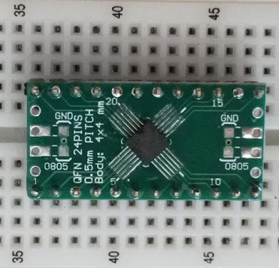
With ever increasing sophistication of microcontroller products, the pin-counts are rapidly rising - so it becomes a challenge on just how to access all of the GPIO pins for breakout, especially when some LQFP packages have 208 pins!

Whilst the extended Arduino headers can handle up to 28 GPIO, clearly another strategy is needed for the larger packages.

From my experience with WiNode, it is very easy to quickly use up several GPIO lines just supporting the on-board peripheral hardware devices:

microSD card        SPI bus +  /CS
RTC                     I2C  + interrupt
SRAM                  SPI + /CS
Keyboard              Clock, Data,
Mouse                  Clock, Data
Wii Nunchuck       I2C
FT812                  SPI, /CS
USB                     UART RX0, TX0
WiFi (ESP-01)      RX1,TX1
RFM69                SPI + /CS + interrupt
Battery Volts        ADC
Battery Temp       ADC

So 20+ lines can easily be consumed with the on board devices.  Incidently, the WiNode 5 has been designed so that it will support other processors in addition to the ATmega1284, in this role it becomes a compact I/O shield.

ARM Challenge

Adopting this format to the larger parts will require a different strategy.  Do we assume that almost all of the "Arduino" pins will be consumed with the local peripherals and that a bus strategy should be employed for inter-board communications?

For ARM packages up to 48 pins, the solution is to craft the device GPIO ports into a 40 pin DIL format, such that it can be plugged directly into the WiNode board. This will take care of the essential system peripherals, leaving the remaining lines available for a bus connector.

On the ARM processors, this is likely to connect directly to the Flexible Memory Controller (FMC). As this is involves a lot of signals, a more dense connector format will be required - and 1.27mm pitch would double the connector density yet remain compatible with 2.54mm standard pitch connectors.

The larger package ARM processors have the FMC external memory controller and also a parallel LCD controller interface - both of which are very intensive in terms of pin usage. These should be routed out to the high density "bus" connectors.

As a rule of thumb - the first three 16 bit ports A, B, C on the ARM will be routed out to 2.54mm headers - based on an Arduino compatible theme.  The higher ports D,E,F,G,  H,I,J & K will be routed to their own double density connectors at either end of the pcb. This format will give maximum flexibility, for the larger pin packages, including memory and FPGA devices.

Trial Fitting a 208 pin processor and a 72Mbit 3nS SRAM

This arrangement will allow unique breakout for up to 156 GPIO signals (The 208 pin STM32F746 or STM32F439BGT6 have a maximum of 166 GPIO lines).

The signals unlikely to leave the board are the clock oscillators PC14, PC15, PH0, PH1,  the JTAG/SWD/ST- link signals PA13, PA14, PA15, PB3, PB4 - which will have their own header.

External Memory Connector.

This 64+4 pin connector handles 32 data lines, 24 address lines and control signals.

LCD Display Connector.

This 64+4 pin connector handles 24 bits of RGB data,  synchronisation signals and pixel clock along with other LCD control signals. It is arranged such that a flexible plastic connector (FPC) common on LCD screens can be easily interfaced .

Clearly a work in progress - the weekends are just to short.


Fignition Revisited

0
0

WiNode plus Evita video board 


Recently I have been thinking again about simple computer systems.  By simple, I mean understandable and those that don't rely on 20 million lines of someone else's code to get to the point that you can have fun with them.

The early 1980s was a very prolific period of design for home computers, especially in the UK, before the very costly IBM PC really took a hold.

Many of these, now 35 year old computers are being revisited and recreated, possibly using new hardware, to create a whole genre of neo-retro machines.

Some History.....

Way back in 2011, I developed an "augmented Arduino" which I called WiNode - a concatenation of Wireless Node.

It featured the ubiquitous ATmega328, an RFM12B 433 wireless transceiver, a real time clock, a microSD connector, a 32kbyte battery backed SPI SRAM and a dual H-bridge for driving small motors and relays.

One of the production batches of WiNode was used in a sound-sculpture installation "Phantom Railings"  at Malet Street Gardens in summer of2012.

About the same time, whilst at Oggcamp 2012, I met Julian Skidmore, who had created a small DIY kit for an 8-bit Forth Computer, called Fignition.

Julian had done a great job in getting it to run a very capable implementation of Forth, and produces audio and video from just an ATmega328.

The Plan.....

Whilst recently reconsidering the role of 8-bit computers, and languages such as Forth, I remembered Julian's work, and WiNode, and wondered whether they might both benefit from an upgrade.

I have subsequently upgraded WiNode to use the much more resource rich ATmega1284, with 16Kof onchip RAM and 128K of flash.  By my reckoning that probably puts it on par with an original 16K Spectrum. However, according to Julian's Forth benchmark figures, when clocked at 16MHz, an ATmega is going to outperform a 3.5MHz Z80A by a factor of about 24.

In the intervening years, Fignition has gained a PS/2 keyboard interface, and is now showing all the signs of a very useful machine for learning to program in Forth. It easily exceeds all the capabilities of the early 1980's Jupiter ACE.

The new WiNode design is a good way of taking the Fignition concept a stage further.   It provides much needed additional RAM capacity,   the super-capacitor backed 32kbyte SPI SRAM can now be used as a persistent store - rather than the main execution RAM  - a much needed speed increase, and the microSD card may be used for removable program storage, put all your favourite Fignition games on uSD and share with your friends.....

WiNode also brings on-board wireless connectivity, either using the RFM69  433MHz or 868MHz low power transceiver, or the plug-in ESP8266 WiFi module.

WiNode by itself is really intended as a stand alone controller, with 28 general purpose I/O lines. The realtime clock, LiPo battery support and non-volatile RAM/uSD card means that it is a good fit for data logging, central heating control, internet connectivity (WiFi) , energy monitoring etc.

However, WiNode 5 has been designed to work with a video generation shield, called Evita, which allows full colour video of up to 1024x768 65Hz resolution via a VGA connection to a large screen monitor.  The Evita board also provides PS/2 keyboard and mouse interfaces, audio output, connection to a LCD touchscreen and also to a joystick or Wii Nunchuck controller. All the right interfaces for a colourful neo-retro computer system.


Experimenting with New Devices - Part 1

0
0
If you were to summarise the developments in microcontrollers over the last few years, you might suggest the movement to 32-bit, mainly through ARM devices, and the rise in open source hardware and software.

Another less well known development is the incorporation of Ferroelectric RAM or FRAM as an alternative to flash memory in the Texas Instruments (TI) range of MSP430 microcontrollers.

Using FRAM instead of Flash memory opens up some interesting possibilities:

FRAM is non-volatile - it retains it's content after power down
It is low power - it can be programmed at low voltages
It has a fast write speed - up to 8Mbytes per second - about 100 times faster than flash
It can be used repeatedly like RAM - it does not wear out after some 10,000 cycles like Flash

Whilst I did gain some experience of the MSP430 some 12 years ago, the introduction of FRAM and modernised peripherals makes them an attractive proposition.

So I decided to invest a little time and money in exploring the new architecture and the new opportunities presented by FRAM technology.

This post and subsequent posts will look at these topics and make a comparison between the more familiar AVR and ARM based devices.

MSP430 Family.

The MSP430 is a 16-bit RISC type microcontroller, with a Von Neuman architecture. This is unusual for microcontrollers (most are Harvard architecture), as it combines both the instruction store and the data store into one unified memory area.

It arose from an early 1990's devices, which was an 8 bit processor, the TSS400-S2, for interfacing to sensors. This early datasheet gives some insight into the heritage from 25 years ago.

The memory architecture is further simplified, as the FRAM and SRAM blocks can essentially be treated as the same codespace for program execution, although execution from RAM is at up to 24MHz, whereas executing from FRAM is limited to 8MHz.

Energia - "Arduino" for the MSP430

The MSP430 range has been supported with low cost "Launch Pad" development boards since 2010, providing an alternative to the AVR or ARM based Arduino or mbed boards. This support extends to the open source Energia IDE project - which is essentially an Arduino compatible IDE (and lookalike) aimed at the various TI microcontroller families. With Energia you can take an existing Arduino sketch and run it directly on MSP430 hardware, with no or few changes. Arduino is certainly becoming a lingua-franca of these small dev-boards.


A look at the MSP430  FRAM devices

The two devices I wanted  to explore are the MSP430FR57xx series and the MSP430FR59xx series.   The MSP430FR5739 is available as as an Experimenter board - below.


The FR57xx series is the smaller of the two with 16Kbytes of FRAM and 1Kbytes of RAM and a maximum clock of 24MHz. It costs about £1.50 in 1off from Farnell and has the potential as being an alternative to Arduino (Nano beater)  - with very few other system components required.  It has 30 GPIO lines which makes it a very good fit for the WiNode 5 format pcb with the extended Arduino headers. Available in a 38pin TSSOP package, which makes it a little easier for home construction.


The FR5969 has 64kB of FRAM, 2K of RAM and a 16MHz clock.

It offers 40 GPIO pins, plus the ability to use both high frequency (16MHz) and low frequency (32768Hz) crystals.

It comes in 40 pin QFN and 48pin QFN packages. A slightly smaller device- with marginally less I/O, the '5959 is available in a 38 pin TSSOP, making it compatible with the '57xx parts but with the beneffit of 64K FRAM and 2K RAM

The MSP430FR5969 is available as the MSP-EXP430FR5969  as a Launch Pad board - for about £12 from Mouser.  This is exceptionally good value, and it has a number of accessory shields available.

Basic Features.

16 bit Von Neuman RISC architecture with 16Kbytes / 64Kbytes  FRAM
16MHz (24MHz *) clock frequency
1.8V to 3.6V operation
100uA/MHz low power operation.
0.25uA RTC
Multiple low power modes of operation
32 bit hardware multiplier
Choice of 10 bit or 12 multichannel ADC
2 UARTS,  SPI, I2C
5 Timers
Low power oscillator
Optional external 32kHz crystal
Optional HF Crystal
16 bit CRC
128 bit/256 bit AES Encryption/decryption processor
31, 33 or 40 GPIO lines depending on package.
Available in 38 pin TSSOP, 40QFN, 48QFN packages.

* Whilst the data sheet says 16MHz, it is perfectly possible to get the digitally controlled oscillator DCO to run at 24MHz. This might be good for a "Turbo-Boost" mode - when power is available.

Datasheet is here.

Tools & Equipment

The Launch Pad and Experimenter boards come with an on-board programmer section, which allows a hex file to be programmed into memory and allows debugging.

The TI Code Composer compiler and tool chain is distributed free of charge for working with these small boards.

If you want to try an open source compiler there is MSPGCC, and if you are seriously into command line hardcore development , you could try  Michael Kohn's  naken_asm which is a cross assembler for a wide variety of microcontrollers.

There are several free tools for loading the hex file into the MSP430. One that I tried is Elprotronics FET Pro-430  Lite  which worked well with the on-board eZ-FET programmer on the launch pad board.

With the above tools I managed to flash a LED using assembly language and also drive a port line at about 2.5MHz square wave.

In Summary & Conclusion

The MSP430 are a fascinating family of microcontrollers. They have utilised every trick to achieve flexibility and very low power operation.  The clocking and low power modes are a study in their own right - but TI through their Launch Pad series of dev boards have made a feature of low power operation - and encourage users to measure the operational current under various modes of working.

Not only is it a 16 bit machine, but it has a universal storage space  - both code and data in one memory - which is all the more interesting for being non-volatile, high speed FRAM.

Although a RISC machine, the ISA is surprisingly versatile with a rich set of instructions and addressing modes.

Just exploring a new instruction set is fun in itself.

The 16 bit architecture is an ideal platform for developing Forth like languages - as these are often based on a 16 bit virtual machine.  Jean-Michel Thooren's "Fast Forth" written in assembly language for the MSP430FR5969 may be of interest to Forth Fans.

Here is a very interesting device - it has a 16 bit architecture, 12 bit A to D and a Von Neuman architecture.  It reminds me a bit of the PDP-8.  More exploration needed.

In Part 2 I'll be looking at porting some existing code to the MSP430 and leveraging some Arduino sketches using Energia.


Experimenting With New Devices - Part 2

0
0
The '5969 Launch Pad  - an ideal experimenting platform for FRAM

In this post I look at ways in which to get the most performance out of a small computer system based around the MSP430FR5xxx with external serial  RAM and FRAM.

MSP430 Performance

The MSP430 being a 16 bit architecture is pitched performance-wise somewhere between AVR and ARM.

If you are doing a lot of 16 bit maths operations, then it will be quicker than the AVR as these are single cycle operations on registers, rather than having to combine two 8 bit operations.

This report compares execution time and code size for a number of common microcontrollers, in particular comparing MSP430 with ARM and AVR.

The speed up factor over an ATmega328 Arduino is as follows:

Simple Maths       1.27
FIR Analysis        3.29
Dhrystone            1.83
Whetstone           2.56

Average               2.24

When this is combined with a 24MHz clock - rather than the normal 16MHz clock on the Arduino the average speed improvement is approximately 3.35.

Code execution is fastest from RAM, so an important speed improvement will be achieved by copying all commonly used code from FRAM to SRAM at initialisation time. This copying process is extremely fast with 1Kbytes of FRAM memory contents copied to SRAM in approximately 128uS.

SIMPL on the MSP430

I tried SIMPL back in 2014 on a very low spec MSP430 value line device in a 20 pin DIL package with only 512 bytes of memory. The C code for SIMPL was compiled using the Energia IDE. There was no difficulty porting what had been an Arduino sketch to Energia - what runs under Arduino runs on an MSP430 under Energia, with zero or very little modification to the sketch. Only the lack of RAM on the MSP430G2553 device was a little problem.

Porting SIMPL to a FRAM Device.

Boosted by the initial success with the MSP430 Launchpad, in getting a basic version of SIMPL to run, I decided to invest in a couple of FRAM based devices.

First, I tried identical sketches on the ATmega328 and the MSP430FR5969.  This was purely so that I could prove that they both ran as expected, and so I could compare the codesize and execution time for each implementation.

For the same clock frequency of 16MHz, the MSP version used about 80% of the codesize and executed simple loops containing integer maths at about 25% improved time.

It was now time to reduce the Arduino supplied UART routines (Serial.xxx) to self coded putchar, getchar and printlong.  This process removed 2200 bytes of code from the implementation - down to 3720 bytes from a starting point of 5920.

The other large chunk of code is the array allocated to holding the initial word definitions. This is a 26 x 48 character array (1248 bytes) - which when removed brings SIMPL down to about 2472 bytes.

The other thing I noticed was that whilst the UART routines take just less than 300 bytes to implement, when they are combined with setup(), the whole thing bloats out to about 640 bytes. This needs further investigation because without this bloating, SIMPL could reside in just 2Kbytes of memory.

Making Use of the FRAM.

The question now is what new features can SIMPL leverage off the back of the MSP430's FRAM?

The write speed of FRAM is well matched to the higher baudrates of the USB to serial converter. Instead of 9600, we can now upload source code at 921600 baud or higher. Using a hex file format, a full 16Kbytes of code could be sent over the serial link in about 0.25 seconds.

The FRAM may be written to at 125nS per 16 bit word, so the whole FRAM storage space could be updated in about 1 milisecond.

The 10 bit ADC could send data back to the PC at almost 100ksps.

Execution from RAM is 3 times faster, so the primitives and the SIMPL kernel are loaded from flash into RAM during initialisation.

The MSP430 has a 20 bit address space, so up to 64 blocks of code could be swapped into FRAM when required.

Off chip storage could be uSD card or even serial FRAM - such as the Cypress 25LV20   which is a 256Kx8 SPI FRAM device in an 8 pin SOIC package.  The SPI bus runs at a maximum of 10Mbit/s - so a "block load" of 1Kbytes is approximately 1mS or the time to load a full 16K block from external FRAM via SPI is 14mS.  This is effectively 1uS access time to a large non-volatile solid state drive.

For faster access either dual SPI or Quad SPI would need to be employed.  This can be done using bit-banging techniques using quite elementary code.

See the Microchip App Note AN1791 for details. A datarate of 8Mbyte/s should be achievable. This would allow the 23LC1024 to be fully read in about 16mS.

To be continued...... soon


Building WiNode 5 - Part 1

0
0
Bare Board, 2 layer, 50mm x 50mm

Two weeks ago, you may remember I finished the pcb layout for a new microcontroller board - WiNode 5  - based on my 50 x 50mm standard board footprint.

Minimum Build.


With mcu, reset and crystal fitted, the board runs "Blink"code


For this I suggest fitting the ATmega1284 SMT package, the 16MHz crystal and its two 22pF capacitors C14 and C15.

Also the 10K reset resistor R1 and the FTDI 6way right-angled header JP1.

A 3.3V  MCP1702 regulator should be fitted in position IC4 along with C2, C4 and C5 its input and output capacitors.

Fit the four 100nF decoupling capacitors around the main microcontroller, C3, C7, C12 and C19.

The 3x2 pin ICSP programming header JP6 should also be fitted.

For LED output fit green LED1 and its 100R series resistor R10.

With this minimum build you may power the board from the FTDI cable and now program the bootloader using ICSP.  If this is successful, loading the blinky sketch should run and the LED should flash.

Now we add the USB chip IC7 (CH340G) the USB connector and the 12MHz USB crystal. Add the 22pf capacitors C18 and C20 and the 100nF decoupling capacitor C20.

Fit capacitors C8, C9  and resistor R2 to provide a filtered AVCC supply.


Add the RFM69 Wireless, the USB and the ESP-01 WiFi

The RFM69 wireless module and the ESP-01 WiFi connector and module can be added at this stage.

Finally - fit the four female shield mounting headers.

Fit the "Arduino" style female socket strips

These allow complete shields to be added, or small modules like the accelerometer module - which is powered by and connected to the Analogue Input port

With axdl 335 Accelerometer module fitted

Programming and Firmware

The Optiboot loader and Arduino "board" files for this project are located at the Mighty1284 Github repository - with more information about the ATmega1284P implentation of Arduino here.

With the new 1284 board files loaded into the hardware directory of the Arduino IDE, you are now ready to program the Optiboot loader into some chips.


Having got the basics of the board in place, and proven that all was working so far, it was at a stage where it could be left  and I could get some sleep.

The final construction stages were to populate the boost converter, fit the FRAM (or SRAM) IC and fit the micro SDcard socket to the underside of the board.

WiNode 5 virtually complete - topside view
Above - the boost converter components, IC, 5 resistors, 2 capacitors and an inductor are added to the lower right corner of the board.

Just above the mcu is the SOIC-8 FRAM IC.

The microSD card socket is added to the underside of the pcb.

And a final word from our sponsors..... Ragworm provided additional boards at no extra charge and couriered them over in time for some weekend fun, as my job is putting the first few boards together.


Building WiNode 5 - Part 2

0
0
Pin Mapping

WiNode 5 is the successor to earlier WiNodes that were based on the 28 pin DIL ATmega328.  

The ATmega1284 offers significantly more features and GPIO pins, 32 compared to the 20 of the ATmega328 - and these all have to be mapped out in a way that makes sense on the PCB. There is also a constraint of 28 header pins - so four of the GPIO appear elsewhere on the pcb - for specific functions - see later.  

There is no common standard, with several commercial ATmega1284 boards doing their own thing - generally based on the 40 pin DIL version of the ATmega1284.

Reverting to good ol' ASCII Art -  Here is one mapping scheme from "Mighty1284P"

//                       +---\/---+
//           (D 0) PB0  1|        |40  PA0 (AI 0 / D24)
//           (D 1) PB1  2|        |39  PA1 (AI 1 / D25)
//      INT2 (D 2) PB2  3|        |38  PA2 (AI 2 / D26)
//       PWM (D 3) PB3  4|        |37  PA3 (AI 3 / D27)
//    PWM/SS (D 4) PB4  5|        |36  PA4 (AI 4 / D28)
//      MOSI (D 5) PB5  6|        |35  PA5 (AI 5 / D29)
//  PWM/MISO (D 6) PB6  7|        |34  PA6 (AI 6 / D30)
//   PWM/SCK (D 7) PB7  8|        |33  PA7 (AI 7 / D31)
//                 RST  9|        |32  AREF
//                 VCC 10|        |31  GND 
//                 GND 11|        |30  AVCC
//               XTAL2 12|        |29  PC7 (D 23)
//               XTAL1 13|        |28  PC6 (D 22)
//      RX0 (D 8)  PD0 14|        |27  PC5 (D 21) TDI
//      TX0 (D 9)  PD1 15|        |26  PC4 (D 20) TDO
// RX1/INT0 (D 10) PD2 16|        |25  PC3 (D 19) TMS
// TX1/INT1 (D 11) PD3 17|        |24  PC2 (D 18) TCK
//      PWM (D 12) PD4 18|        |23  PC1 (D 17) SDA
//      PWM (D 13) PD5 19|        |22  PC0 (D 16) SCL
//      PWM (D 14) PD6 20|        |21  PD7 (D 15) PWM
//                       +--------+

This is a fairly logical approach, with pins numbered starting from Pin 1 of the package and just following the package around.  However it does not tie in well with the mapping on the Arduino or WiNode 5 board:

The Bobuino pin mapping is much more like the original Arduino - preserving D0 to D13 in their old familiar positions and functions, plus the analogue inputs mapped to D14 to D21, and the additional (Port C) pins following on as D22 to D29. This just puts SCL and SDA a little bit off beat as D22 and D23.  The mapping scheme is better but not perfect:

//
//                       +---\/---+
//           (D 4) PB0 1 |        | 40 PA0 (D 21) AI 7
//           (D 5) PB1 2 |        | 39 PA1 (D 20) AI 6
//      INT2 (D 6) PB2 3 |        | 38 PA2 (D 19) AI 5
//       PWM (D 7) PB3 4 |        | 37 PA3 (D 18) AI 4
//   PWM/SS (D 10) PB4 5 |        | 36 PA4 (D 17) AI 3
//     MOSI (D 11) PB5 6 |        | 35 PA5 (D 16) AI 2
// PWM/MISO (D 12) PB6 7 |        | 34 PA6 (D 15) AI 1
//  PWM/SCK (D 13) PB7 8 |        | 33 PA7 (D 14) AI 0
//                 RST 9 |        | 32 AREF
//                VCC 10 |        | 31 GND 
//                GND 11 |        | 30 AVCC
//              XTAL2 12 |        | 29 PC7 (D 29) 
//              XTAL1 13 |        | 28 PC6 (D 28) 
//      RX0 (D 0) PD0 14 |        | 27 PC5 (D 27) TDI
//      TX0 (D 1) PD1 15 |        | 26 PC4 (D 26) TDO
// INT0 RX1 (D 2) PD2 16 |        | 25 PC3 (D 25) TMS
// INT1 TX1 (D 3) PD3 17 |        | 24 PC2 (D 24) TCK
//     PWM (D 30) PD4 18 |        | 23 PC1 (D 23) SDA
//      PWM (D 8) PD5 19 |        | 22 PC0 (D 22) SCL
//      PWM (D 9) PD6 20 |        | 21 PD7 (D 31) PWM

//                       +--------+

My problem is that pins B0 and B1 are not routed to the regular headers but appear on the upper H-bridge connector JP4 and the "X-Bee" shield. Additionally Analogue inputs A6 and A7 are used on board for battery volts and battery temperature monitoring. These rogue pins need to be accounted for in the mapping scheme.This therefore gives rise to the modified arrangement:

//
//                       +---\/---+
//            (D 30) PB0 1 |        | 40 PA0 (D 22) AI 0
//            (D 31) PB1 2 |        | 39 PA1 (D 23) AI 1
//        INT2 (D 8) PB2 3 |        | 38 PA2 (D 14) AI 2
//      PWM0A  (D 9) PB3 4 |        | 37 PA3 (D 25) AI 3
//   PWM0B/SS (D 10) PB4 5 |        | 36 PA4 (D 26) AI 4
//       MOSI (D 11) PB5 6 |        | 35 PA5 (D 27) AI 5
// PWM3A/MISO (D 12) PB6 7 |        | 34 PA6 (D 28) AI 6
//  PWM3B/SCK (D 13) PB7 8 |        | 33 PA7 (D 29) AI 7
//                   RST 9 |        | 32 AREF
//                  VCC 10 |        | 31 GND 
//                  GND 11 |        | 30 AVCC
//                XTAL2 12 |        | 29 PC7 (D 21) 
//                XTAL1 13 |        | 28 PC6 (D 20) 
//        RX0 (D 0) PD0 14 |        | 27 PC5 (D 19) TDI
//        TX0 (D 1) PD1 15 |        | 26 PC4 (D 18) TDO
//   INT0 RX1 (D 2) PD2 16 |        | 25 PC3 (D 17) TMS
//   INT1 TX1 (D 3) PD3 17 |        | 24 PC2 (D 16) TCK
//      PWM1B (D 4) PD4 18 |        | 23 PC1 (D 14) SDA
//      PWM1A (D 5) PD5 19 |        | 22 PC0 (D 15) SCL
//      PWM2B (D 6) PD6 20 |        | 21 PD7 (D 7)  PWM2A

//                         +--------+ 


With any pin-mapping , it is clearly a compromise between physical and logical arrangement. These changes can be incorporated into the pins_arduino.h header file. We achieve a mapping that is reasonably familiar with existing Arduino pin-out and ties in well with the physical layout of the pcb:


//                   _________________________________
//        RXD0 (D0) |o            A7  (D29)          o|A5  (D27)
//        TXD0 (D1) |o            A6  (D28)          o|A5  (D26)
//   RXD1 INT0 (D2) |o            B0  (D30)          o|A3  (D25)
//   TXD1 INT1 (D3) |o            B1  (D31)          o|A2  (D24)
//       PWM1B (D4) |o                               o|A1  (D23)
//       PWM1A (D5) |o                               o|A0  (D22)
//       PWM2B (D6) |o                                |
//       PWM2A (D7) |o                                |
//                  |                                o|VIN
//       INT2  (D8) |o                               o|0V
//      PWM0A  (D9) |o                               o|0V
//   PWM0B/SS (D10) |o                               o|+3V3
//       MOSI (D11) |o                               o|+5V
// PWM3A MISO (D12) |o                               o|RES
// PWM3B  SCK (D12) |o                               o|C5  (D21)
//         0V       |o                               o|C4  (D20) 
//       AREF       |o         Open Hardware         o|C3  (D19)
//        SDA (D14) |o            WiNode 5           o|C2  (D18)
//        SCL (D15) |o                               o|C1  (D17)
//        ANT       |O                               o|C0  (D16) 
//                  |_________________________________|


This makes for a neat, logical arrangement, where the pairs of complimentary PWM outputs are located next to one another - and in a neat group D4-D7.

SCL and SDA are on the end of the upper digitals - where you would expect them on an R3 shield.  

The JTAG lines (TCK,TMS, TDI,TD0) are in a neat group on the extended headers C0-C5.  C4 and C5 may be used for active signalling to the shield through the Arduino I/O and NC pins on the end of the power header.

ANT is the antenna connection to the RFM69 wireless transceiver module.


In part 3 we further name and map these pins to suit the EVITA graphics shield and the Open Inverter H-bridge module.

Building WiNode 5 - Part 3

0
0


Some five years have passed since the original WiNode design, and WiNode 5 - consider it to be the Anniversary Edition, has tried to build upon some of the changes that have happened over the intervening years. There has been an explosion of low cost wireless modules onto the hobbyist market, WiFi, Bluetooth Low Energy (BLE) and upgraded
More than just an ATmega1284 Platform

WiNode comes towards the end of my involvement with 8-bit microcontrollers - as I move towards 16 bit and 32-bit devices. For this reason it was designed with future proofing in mind.

Whilst a surface mounted ATmega1284 may be soldered to the pcb for the basic board, there is also provision for a 40 pin DIL socket or pair of female header strips to be fitted down the centre of the pcb.  If the ATmega1284 is not fitted to the board, then any other mcu of up to about a 48 pin package - suitably mounted on a small carrier pcb that matches the 40 DIL pin-out,  may be plugged into the board. The 40 pin "socket" is based around the pin-out of the DIL ATmega1284 - so even one of those can be fitted if necessary.

This technique allows the use of a range of small processors, including ARM Cortex M, MSP430 and the like. I already have prototype designs for STM32Fxxx and MSP430 microcontroller variants.

With the upgrade in processor, comes an increase in clock frequency, increase in memory, improvement in peripheral features and speed and often an increase in ADC resolution.

ARM Cortex M4 Variant

For instance, the STM32F373 - a 72MHz ARM Cortex M4 in a 48 pin LQFP package comes with 3 UARTS, 2 SPI, 2 I2C,  up to 256Kbytes of Flash and up to 32Kbytes of RAM, plus a multichannel  12 bit ADC and 3 separate differential input Sigma Delta 16 bit ADCs. The Cortex M4F core comes with floating point and DSP operations. This is the ideal processor for high speed manipulation of analogue sampled data - for example 3 phase energy monitoring.  These processors start at £3.33 in 1 off.

MSP430 Variant

Another interesting processor is the ultra low power MSP430 FR series.  These are a 16 bit processor with 24MHz clock frequency, 12 bit ADC channels, 2 UARTs, SPI and I2C.  The unique feature of the FR series is that they use non-volatile ferroelectric FRAM memory for program and data storage. This allows exceptionally low power operation, retaining data after power down and capable of very fast write access - for high speed programming or datalogging.

Other Interesting Options

There is an increased interest in the use of FPGAs as a means of providing open source soft core processors.  One such option is the J1 Forth processor implemented on a low cost Lattice FPGA - using an open source toolchain.  The FPGA is available in an 84 QFN package just 7mm x 7mm which could be fitted onto the DIL 40 carrier board.


The WiNode 5 Hardware and Peripherals

Here I describe the hardware in a little more detail:

All of the hardware on WiNode 5 is designed to work at a 3.3V Vcc - thus keeping power requirements to a minimum.  Think carefully before you connect to any non- 3.3V shield!

The RFM69 wireless transceiver is still very much fundamental to the design, tracing it's roots to Jean Claude Wippler's JeeNode design - which used the ATmega328 and the RFM12B - and was probably about one of the first commercial wireless connected Arduino variants.

The RFM69 uses D10 for it's chip select, and the new INT2 interrupt that is available on the ATmega1284 - appearing on D8.

In addition to the encumbent RFM69, WiNode 5 also offers an un-committed "X-Bee" footprint (XB1)  This allows any additional wireless device to be added at a later date - based on a shield that conforms to the X-Bee pinout.

One of the biggest advances in the last 2 years is the emergence of very low cost WiFi modules based on the ESP8266 device. WiNode provides a 4x2 connector to allow an optional ESP-01 WiFi module to be plugged in directly so that it can communicate with the mcu using the additional UART 1. Note that WiFi support is optional and not central to the WiNode philosophy. Using a pre-built mass-produced plug-in module is the quickest and cheapest way to give it WiFi connectivity.

The original WiNode used a non-volatile 32Kbyte 23K256 SPI SRAM - backed up by a small super-capacitor.  This feature has also been retained with IC3 a SOIC-8 package, but now the device can be an SRAM of up to 128Kbytes or a ferrroelectric FRAM of up to 256Kbytes. Chip selection is by port B0.

Whilst novel when first introduced on my Nanode RF design of 2011, the micro SD is now common place on many development boards and SBCs.  I have retained the same basic uSD socket - soldered to the underside of the pcb and selected using port D9.

With lower power, yet more capable microcontrollers, there is frequently the need to make portable battery powered devices.  With the emergence of cheap Lithium polymer (LiPo) battery technology, WiNode 5 reflects this with support for an external battery.  This does not need to be a LiPo as an on-board boost converter, IC6, based on low cost MCP1640 allows a single cell to be boosted up to 3V3 so as to power the board.

One of the biggest bug-bears 5 years ago was the crippling cost of placing an FT232R device onto the board in order to allow connection to a PC via USB. Fortunately there are now several much lower cost alternatives available, and WiNode 5 uses the CH340G device in position IC7 - which is available for less that $0.50. It needs a 12MHz crystal  Y3 for correct USB timing.

The ATmega1284 provides a whole additional 8 bit port over and above what the ATmega328 supplies.  Six of these additional port lines are broken out to a header which is placed below the usual 6 pin Arduino "Power" header.  These additional pins are general purpose I/O, but also carry the signals associated with the JTAG interface.

As WiNode 5 uses several SPI devices, the additional port lines C0-C5 can be used to select additional devices on the SPI bus - this offers an easy route for expansion. More on expansion later.


Board Pin Out Details

WiNode 5 has been designed to act either as a stand alone, battery powered, wireless connected controller or monitor,  alternatively as part of a larger system.


//                    _________________________________
//      PC-RXD0 (D0) |o            A7  (D29)          o|A5  (D27)
//      PC-TXD0 (D1) |o            A6  (D28)          o|A5  (D26)
//   * ESP-RXD1 (D2) |o            B0  (D30)          o|A3  (D25)
//   * ESP-TXD1 (D3) |o            B1  (D31)          o|A2  (D24)
//     KBD_DATA (D4) |o                               o|A1  (D23)
//           PD (D5) |o                               o|A0  (D22)
//    MOUSE_CLK (D6) |o                                |
//   MOUSE_DATA (D7) |o                                |
//                   |                                o|VIN
//    RFM_INT2  (D8) |o                               o|0V
//      uSD_CS  (D9) |o                               o|0V
//      RFM_CS (D10) |o                               o|+3V3
//        MOSI (D11) |o                               o|+5V
//        MISO (D12) |o                               o|RES
//         SCK (D12) |o                               o|C5  (D21)
//          0V       |o                               o|C4  (D20)
//        AREF       |o         Open Hardware         o|C3  (D19)
//     I2C-SDA (D14) |o            WiNode 5           o|C2  (D18)
//     I2C-SCL (D15) |o                               o|C1  (D17)
//         ANT       |O                               o|C0  (D16)
//                   |_________________________________|


One of the first applications is that of a retro-computer system using the EVITA graphics driver board (above).  EVITA provides 1024x768 full 24bit colour graphics and an interface for PS/2 keyboard and mouse. It also allows a Wii Nunchuck controller to be plugged in.

With just WiNode 5 and EVITA, you have a complete retro-computing work/play station capable of driving a large screen monitor in just 2 small pcbs.  For portability you can use a Gameduino2 shield and a LiPo battery.

The slight conflict yet to be resolved here is when using the PS/2 keyboard with the ESP-01 WiFi. The keyboard generates a clock which needs to interrupt the mcu via INT1 (D3).

If used with a Gameduino 2 - INT 0 (D2) is also required. This kind of precludes the use of the ESP-01 WiFi - unless a work around is possible.

PCB Layout

WiNode was designed from the start to be smaller than the standard Arduino (Uno) - always considered to be too bulky and "Arty" rather than a simple rectangular board with sensible pin spacing and mounting holes. At 55x64mm it was intended to fit into a readily available plastic case with a battery enclosure. WiNode used predominantly through hod mounted components wherever possible.

WiNode 5 takes advantage of surface mounted components - as it was found that even the through hole parts presented too much of a soldering challenge to the average user.  This means that the circuitry can have a greater density - thus a smaller pcb and be cheaper to assemble - using pick and place machines and reflow soldering ovens.  It is really geared up for the modern electronics pcb assembly processes.  As a result, WiNode 5 packs a lot more functionality into a 50mm x 50mm pcb - some 71% of the board area of it's predecessor.

Whilst WiNode 5 can be hand soldered - it will take a few hours and you really need to be proficient at surface mount detailed soldering, have good light and good magnification available.

The board is based on a 50 mm x 50 mm standard footprint - with the aim of retaining Arduino header compatibility on the smallest pcb possible.   WiNode takes advantage of pre-built plug in modules - such as the ESP-01, the adxl 335 accelerometer module and the X-Bee module.  These can be bought on ebay cheaper than they can be built.1ghz>

The Great MSP430 Bootloader Swindle

0
0
Bootloading Blues.


The MSP430 is a great little micro, and with some proper marketing, it could easily have provided an alternative to the AVR and PIC.  However unclear, obfuscating, archaic documentation, spread very thinly over the web has made this little micro the poor relation of the microcontroller world.

I write this having just spend a considerable amount of time in February trying to provide an effective solution for programming one of our products, an MSP430 based force gauge, which is being produced by a new supplier.

Unfortunately the original programmer from Gessler is no longer available, and so an alternative was needed.

The solution was actually staring in me in the face - so simple, that it's elegance seems to have been lost in the mists of time, and the desire to make everything a lot more complicated than it needs to be.

Here I summarise my findings in an attempt to provide a reference that will allow others to benefit from my 3 weeks of frustrating work and false starts.

AS a prologue to the main post - here is an unpublished post from 3 weeks ago - when I first started on this mission

(Previously unpublished - from Feb 9th 2016)


We have an on-going project at work, which needs an MSP430 bootloading over it's serial port with a hex file.  So we went out and bought the cheap open source, Rocket BSL programmer from Olimex.

I then found that I needed the drivers and other software from TI,  which I had to register for and then declare to the US Government that I wasn't going to use it against America in any way, shape or form.  So far, so good.

North Korean? No, just Bulgarian.
The MSP430-BSL is described as a joint project between Olimex and Texas Instruments. The reality is that no-one really wants to take ownership of it, and there is no one specific site that you can go to that gives you everything you need to get this programmer to work.  It's like the code has been fragmented and spread to the four corners of the known cyber world - lest anyone dares try put the fragments together again and unleash the awesomeness of this great force on mankind. What I'm trying to say is that both Olimex and the Mighty TI have this time shot themselves in both feet, and it's no surprise that the MSP430  is languishing in some stagnant microcontroller cul-de-sac.

After mulling this over for a while, I began to think that proprietary bootloaders often really suck. There should be a simple, low cost universal tool which allows you to squirt code from a hex file into any microcontroller, from any platform.  And that got me thinking about the humble USB-serial programming cable - such as those by FTDI, SiLabs or our Chinese friends who make the CH340.

It also appears that others have had this thought.  In my search for an alternative MSP430 programmer, I found this interesting approach from Flying Camp Design - a programmer that is literally not much more complicated than an FTDI cable - just an FT232R on a small pcb.

Bootloaders are usually designed to be small, and not particularly human-friendly, because they are normally talking to some proprietary application running on the pc.  But this doesn't need to be the case, there is sufficient flash space in the boot block of most micros to put a more sophisticated bootloader program - one which is actually capable of running some interpreted commands and presenting a more human friendly face to the user.


Getting Started

The MSP may be programmed by one or more of the following interfaces:

1.  A Serial Boot Loader - resident on all MSP430 devices - known as BSL
2.  A JTAG interface/programmer
3.   SpyByWire  - a 2 wire serialised version of JTAG.


The Electrical Interface

Our force gauge product has a 6 pin connector on board intended for a BSL programmer.  This has  the following signals present - wired to pins on the IC:

TX
RX
TEST
RESET
0V
VCC

A combination of signals on the test and reset pins puts the device into bootloader mode.  The data is then sent by the PC and received by the Rx pin and acknowledged by the Tx pin.

The Spec Document

The bootloader is fairly well specified in TI's document SLAU319 - and for anyone wishing to understand the bootloader, this should be the starting place.

When the MSP430 was first designed, the engineers made available a small bootloader program, residing in protected ROM, which allowed serial communication directly to a PC via a couple of pins. The BSL interface also allows you to read the contents of the Flash, erase it, verify and a range of other commands - some protected by a password mechanism  - so as to avoid illegal copying of protected IP.

Towards the middle of the SLAU319 document, a circuit for a programming interface is provided:

This circuit dates from the early 2000's  - when all PCs and laptops came with 9 pin serial COM ports.

In essence, there are three, level shifted outputs from the COM port to the target device, and one level shifted input back to the PC. Modern RS232 generally puts out +/-6V - and we need 0-3V TTL levels for the MSP430.  The circuit is powered by harvesting spare energy from the output lines through diodes and pumping up  a capacitor. The raw supply feeds the TL062 op-amp and  is then regulated to 3V to provide a stable supply for the 74AHC14 Schmitt inverters.

This really is a very simple circuit - but sadly off-putting because it uses about 25 components and uses the now obsolete  9 way D-type and COM port.

What is really needed is a modern equivalent that works with USB and modern software drivers.


USB Implementation.

There are several low cost USB to serial converter chips to choose from, including FTDI, CP2102 (SiLabs) and the newer Chinese CH340G.  All of them have the potential to work in this circuit.

I covered the CH340G in a recent post and the datasheet is here. The CH340 is low cost and easy to use. I have subsequently used the CH340G on some of my other projects.

For my experimentation, however, I used a  SiLabs CP2102 device mounted on a small pcb - solely because I had it lying about.  It breaks out all of the common RS232 signals - including RTS and DTR which we need.   These modular devices are available from ebay for a couple of dollars - and a variety to choose from.

CP2102 module by Baite Electronics 
The one above comes with a set of double ended leads - so you can easily make up your own custom cable.


So to make this work we need to access Tx, Rx, RTS and DTR.  RTS and DTR are often available on the 4 way headers down the side of the module.

The module also conveniently supplies a 3V3 supply from an internal voltage regulator (see datasheet) - this can supply a maximum of 100mA - more than enough for powering most MSP430 dev-boards.

Programming Application Software

I tried a couple of programming applications, with very little success - until I stumbled MSPFET - from a Russian gentleman Kurt. This did exactly what was needed - allowing a hex file to be loaded into the MSP430.


Programming the MSP430 really is that cheap and easy - using free software and a USB to serial module costing under $2 - finding out how to do it -  from the information spread over the web it - was so very much harder.

Common Myths - Busted

You don't need a $300 JTAG Programmer. In desperation I found a FET-Pro 430 reduced to $50 on ebay.

You don't need an $11 Olimex MSP-BSP "Rocket" Programmer. I bought two of these from Mouser - I am still trying to find the correct software to make them work.


In conclusion

The BSL feature that comes with almost all MSP430 devices is great at doing what it was intended for - a very simple means of getting your hex file into the MSP430's flash.

The resources needed to make this work are trivial, and it could make a great addition to any application that needs the ability to modify the flash memory.

Unfortunately, the documentation has been obfuscated and made more compex than needs-be by JTAG and SpyByWire (for debugging) - and so few people are aware what a simple facility BSL is to use.  The hardware needed in the form of a USB - Serial converter should be part of every hobbyist's or Engineer's toolkit.

The resources needed to make this work are trivial, and it could make a great addition to any application that needs the ability to modify the flash memory.

The protocol is simple, as is the 2 signal start-up sequence -  and at a pinch, if you didn't have a serial converter that supports DTR (eg FTDI cable) you could hack an Arduino or Launchpad to generate the start-up sequence. You could even make a standalone programmer for repeat programming of boards out in the field using a Launchpad.

Energia has made the MSP430 more accessible - providing an Arduino like development environment. However, it is still nice to know how the simple low-level bootloader scheme works.


More MSP430 Machinations

0
0
In the last few weeks I have been acquainting myself with the MSP430  - as a possible low cost candidate for future projects.

There are literally hundreds of different variations of the MSP430 - and to the newcomer the range of devices can appear to be quite daunting.

However, for my initial experiments I have been looking at some of the low end devices - which are particularly accessible in terms of very low cost and ease of use - and available for the MSP430G2XX Launchpad dev-board.

The low-end devices are interesting because of their low cost and flexibility of peripherals, and the combination of a 16 bit ADC and a high speed universal serial peripheral makes for some novel sensor applications - particularly when applied to strain gauge, loadcell and barometric sensors.

Low Cost Hardware -  and Free CCS Compiler

This entry level Launchpad is available for about £7 (US$11).  It comes with integrated programmer/debugger and will accept most of the DIL packaged MSP430 ICs.  The free to use Code Composer Studio IDE, consisting of compiler, debugger and other workbench tools may be downloaded from the TI website - after a registration process has been completed.  TI has produced dozens of useful code examples - which are a great way to learn the programming techniques of these devices.


The all round work-horse shipped with the Launchpad is the MSP430G2553 which comes in a 20 pin DIL package and has 16K of program space, but only 512 bytes of RAM.  There is also, included with the Launchpad kit an MSP430F2542 with 8K of codespace but only 256 bytes of RAM.
The MSP430G2553 does have a proper uart - but for BSL purposes Rx is on Port 1.5 and Tx is on Port 1.1.

The other device of current interest is the 14 pin DIL MSP430F2013 - which is a very low cost device but it's unique point of interest is that it is one of the few devices that has a 16 bit SD_16 A ADC and is ideal for sensor applications. However it has even less Flash (2K) and only 128 bytes of RAM! There is however 256 bytes of "Information RAM" - which is handy for storing device identity, calibration factors etc.

According to TI literature, the MSP430F2013 comes with a uart based bootloader (BSL). This is curious, and yet to be fully confirmed,  as the uart is one hardware peripheral missing from the '2013!

There is a RAM based software BSL described in application note  SLAA450

These small devices are all resource limited, but as such inspire ingenuity. Programming code for these is not-dissimilar to what programming the first generation microprocessors was like 40 years ago,  but with  moderately fast 16-bit, very low power processor plus uart or universal serial interface built in.

SIMPL Revisted 

On small devices with perhaps only 2K bytes of flash memory available, I have revisited my implementation of SIMPL on the MSP430, as until now, I have focussed on AVR and ARM implementations.  With a bit of help from online code examples - I have managed to eliminate much of the code intensive remnants of "Arduino" and shoehorned  a full featured version of SIMPL into just 1868 bytes, putting it well within my self-imposed 2Kbyte limit. This makes it applicable to the '2013, '2452 and '2553 devices.

With additional functionality and further code optimisation then a 2K limit seems a reasonable size for the SIMPL kernel, especially if there is bootloader support included.

The code for the MSP430G2553 version is here on this Github Gist

I have implemented a 10 bit ADC on P1.3 which is read using the s (sample) command.  To read 1000 consecutive ADC samples at 100mS intervals, the following code snippet of a sampling loop with delay can be used

1000{sq100m}

q prints the output of the ADC followed by a crlf.

With a bit of ingenuity it's possible to build up a horizontal bar graph display - of line length proportional to the input on the ADC.


:B  s{_[_}q

Sample the ADC using s and print the corresponding number of brackets along a line. The final q prints the ADC value followed by a crlf.

SIMPLy Short of RAM

The smaller MSP430 parts are really quite short of memory with some only 256 or 512 bytes available.  This really is a limitation when it comes to writing sketches in an interpreted language, so one possible solution is to add a serially accessed SRAM (or FRAM) on the SPI bus.  This will extend the available memory to 32Kx8, 128K x 8 or even 256K x 8 in fast access non-volatile FRAM - (if your budget permits).

MSP enthusiast, Rick Kimball  has written a library to access the 23K256.  A single byte can be accessed in 98uS, but the full 32Kbytes can be streamed in 100mS.

The beauty of the SPI addressed memory devices is that they interface using just 4 pins - ideal for low pinout devices such as the '2013 and '2553.


A Historical Note on Memory.

Ever since the Manchester "Baby" the 1948 small scale experimental computer, the operation of the cpu has been intimately tied to the operating characteristics of the memory.  The computer has essentially been designed around the best memory solution available at the time, be it Williams CRT Tubes,  mercury delay lines, dekatron tubes or magnetic core memory.  The PDP-5 and PDP-8 were designed specifically around the most economical core memory available in the mid-1960s - even though it took half a rack of circuit modules to interface to the core.

In some ways, the little computer that I am proposing, is the modern day equivalent of the PDP-8 (or possibly the 16 bit PDP-11). It is a compact 16 bit von Neuman architecture cpu with limited on chip storage, tied to a serial RAM, which can be efficiently accessed in pages or blocks of 32 bytes.

Within SIMPL it should be possible to write some User words to access the off chip serial RAM in an efficient manner - perhaps treating it like a virtual disk.


Next time - serial communications.


MSP430 Serial Communications

0
0
Fun with the MSP430F2013.

I have been playing about with the MSP430F2013 for a couple of days now - and finding out what a wonderful little microcontroller it can be.

It really is short of both flash memory and RAM (2K and 128 bytes respectively) - so applications have to be very compact. However it makes up for these shortcomings with some very useful and flexible hardware.

My first application is to use it as a lower cost alternative to an AD7767 ADC which I currently use in a loadcell interface.

Although it does not have an on-chip 24 bit ADC, the output resolution of the SD_16 ADC should be sufficient for my immediate needs. This little $1.50 mcu already saves me $10 on not having to buy an AD7767 then service it with another mcu.

The second useful peripheral is the Universal Serial Interface (USI) - this is a flexible device used for both I2C and SPI communications, and as will be seen below later can also be used for high speed asynchronous uart communications too.

Using the USI

The universal serial interface is a flexible peripheral that is primarily intended to automate the processing of SPI and I2C communications. With a bit of bit-banging trickery - to add start and stop bits, it can also be used as a Transmit UART.  Rick Kimball has also experimented with high speed asynchronous serial from the USI - which is capable of a massive 16Mbaud - but I doubt anything much over 3Mbaud will be accepted over a FTDI cable!

By way of a test, I hacked together a quick routing to read the ADC and send its 16 bit sample to the USI.
At it's heart it has a variable length shift register which can shift a maximum of 16 bits. By adding in a start and stop bit, and setting the shift register length to 10 bits, the USI has no problem sending asynchronous serial data at up to 2Mbaud.

With potential serial at the processor full speed - SPI transfer at 16MHz should be possible - and it's definitely worth trying.

This will allow word length transfers to be made with the serial SRAM, and will be more efficient it setting up longer addresses.

The SRAM needs a 32 bit control packet to be sent prior to any transfer.  This consists of an 8 bit instruction followed by a 24 bit address.  The RAM handler code should be able to efficiently set this up and clock it out  to the SRAM as two consecutive 16 bit transfers. From there on it just emits clocks (dummy bytes) to accept the data bytes from the RAM. On long sequential transfers about 300Kbytes per second transfers should be possible.

MSPEZIO

This is a collection of useful I/O functions to make your programming life a whole lot easier. Written for physics students at the University of East Carolina. I quote:

This guide is intended to serve as a fast introduction to the use of the msp430x2xx embedded microcontroller for use by students in Electronics and Advanced Laboratory environments. The intent is to allow an easy access to calls for I/O applications and serial communications transmitting data to external computers. It is assumed that the student has some understanding of c-programming and has been through the introduction to using the Code Composer Studio or IAR Embedded Workbench Kickstart, IDE’s. 

16 Bit ADC

With code based on one of the mspezio examples, I was quickly able to get the SD16 ADC working and sending data out of a bit banged uart. MSPEZIO offers several examples that can be tried with CCS on the basic LaunchPad hardware.

The SD16 ADC is quite comprehensive - and the mspezio set-up made the initialisation of this peripheral a lot easier.  I was able to set it up to read a strain-gauge based loadcell and send readings to the PC terminal application.  The MSP430F2013 really only has just enough pins to allow a simple loadcell interface with serial comms.  The output of the ADC values can be triggered by sending any character over the serial comms   - using the mspezio WaitForSerial() function.

Much of the progress I have made with the MSP430 has been the result of evenings and weekends looking online at other code examples and good old experimentation.  By modern standards the MSP430 is not a complex microcontroller, requiring significantly less initialisation code to get the basics working.  I would recommend buying a Launch Pad to anyone who wants to tinker with something a bit different.  As stated in a previous post, the board is low cost and there is free access to the CCS Code Composer Studio compiler and also the Arduino like Energia IDE.  CCS offers multiple file projects to be built and debugged whilst Energia allows easy entry level to simple sketches.


SIMPL on MSP430F2013

The plan now is to get Energia working with the MSP430F2013 so as to allow a cut down version of SIMPL to be run on it.

Energia allows the SIMPL application to be built up a routine at a time - so that every last byte of precious code space can be efficiently used. This is very important on the '2013 - which only has 2K codespace and 128 bytes of RAM!

The biggest problem with the MSP430F2013 is that it does not have a proper uart peripheral and whilst uart transmit is possible using the USI module with a bit of  trickery, the uart receive function becomes a major challenge - involving either a timer controlled sampling of the incoming bit stream or something as yet unknown.

The porting of SIMPL and the MSPEZIO helper functions to the '2013 will be the subject of a forthcoming post.


More Nano Computing - The "Universal Microcontroller"

0
0
In this post I discuss the idea of a "Universal Microcontroller" - a 40 pin plug in module that can host mcus from a variety of different manufacturers and families.  It is based around a standard 40 pin 0.6" wide DIL footprint for convenience and low cost.

The impetus behind this concept is caused by the fact that there are dozens of new microcontrollers appearing on the market every year and by having a common, low cost easy to use module would be a good way to evaluate some of the various product offerings in a breadboard friendly format.

Selecting a Small Microcontroller

There are so many selection criteria - so I will try to target a few of the more important ones

RAM
ROM

POWER
PERIPHERALS

SPEED
SIZE

COST
COMPILER
COMMUNITY

RAM/ROM  - these relate to the size of the on chip memory allocations.  Most microcontrollers these days tend to have a lot of flash ROM and a lesser amount of RAM.

If you are handling arrays and buffers, then RAM is important - and it is very easy to run short if your device has 2K or less. (Notably Arduino ATmega328).

There are a whole class of tiny microcontrollers, which have less than 1K bytes of RAM.  It is more difficult to use these for general purpose applications - and they tend to be used for deeply embedded low end consumer goods, sensors etc.

POWER

A lot of applications for microcontrollers have to be battery powered - so there is a large emphasis on tailoring the application in such a way that battery life is maximised  - particularly if you are operating from a coin cell or similar. Some microcontrollers are very power efficient, and have multiple low power modes including low voltage operation.

PERIPHERALS

The microcontroller manufacturer chooses to fit-out a particular cpu core with a certain set of peripherals and it is these which give the microcontroller it's flexibility and capability in handling various applications. An mcu which is lacking a particular peripheral can be very difficult or impossible to match well to a particular application. A rich peripheral set often minimises the amount of glue-circuitry needed to interface to common external devices.

Peripherals may be grouped as follows:

Communications   UART  SPI  I2C USB etc
Timing     TIM
Driving    PWM
Sensing   ADC  DAC  Comparator
Misc       GPIO

These are the basic building blocks - the larger mcus may have sophisticated peripherals for audio, LCD video and external memory interfaces.

SPEED

The clock frequency of microcontrollers has increased steadily over recent years - and many have sophisticated clock control options to allow variable frequency clocking schemes especially for low power operation at much reduced frequency.

Most modern, general purpose microcontrollers will run at up to 20MHz or so.  From then on upwards it could be best described as following a 1,2,5 progression:

20MHz            AVR   MSP430  ARM M0
50MHz            ARM Cortex M0+
100MHz          ARM Cortex M3/M4
200MHz          ARM Cortex M4/M7
500MHz          ARM


SIZE

This refers to the word size used by the mcu. Originally dominated by the 8-bit families (PIC, AVR, 8051 etc) these low end microcontrollers are being replaced by much more capable and cost-effective 32 bit parts, generally based on the ARM architecture. The 16bit MSP430 is an interesting exception -and will be interesting to see how this family product line fares in the face of competition from ARM.  TI have already brought out their own  MSP432 range based on 32bit ARM Cortex M4F cores.

COST

Microcontrollers range in cost from about 35 cents to about $12.  These will have flash memory sizes from 512bytes to 2Mbytes and clock speeds that range from 20MHz to over 200MHz.  Package sizes from just 6 pins to over 200 pins. Again it might be worth imposing a 1,2,5 scale on your budget - and see just what parts match your requirements.

COMPILER

This is a big factor in choosing a microcontroller.   Can I program it easily, and how much does the tool chain cost?  Fortunately there are free tools available - including code-size limited or time limited evaluation versions of some of the professional tools.  The open source community has done a lot to make microcontrollers more accessible.

COMMUNITY

This has become increasingly important. Is there a good online help forum where beginners can get advice. Is the chosen device well supported by a community?


The Universal Microcontroller

Having selected our microcontroller how do we achieve universality?

About a month ago I reviewed a low cost version of the "Arduino" Nano - made in China using the CH340G USB to serial converter IC. The Nano has a lot going for it  - in terms of low cost and compact size.  The DIL format makes it easy to use.  However it's 8 bit mcu is now showing it's age - especially when there are cheaper, faster and more feature rich 16bit and 32bit mcus available.

Other processors also use this DIL format - such as the "Maple Mini" based on the STM32F103, and my own "ARMiGo" based on the STM32F373 (with 3 x 16 bit differential input ADCS).

Looking further afield there are the Teensy series of boards based on the Freescale (now NXP) MK20DX series of ARM Cortex M4 mcus, and McHCK! also based on the MK20DX series.

I am also more interested in the MSP430 reange of 16 bit microcontrolers - now that they have FRAM memory - and are fully supported by Energia - an Arduino IDE "workalike" for the MSP430 and other TI processors.

Is there a Universal module format that can accept all these different devices?  My mission now is to try to develop one

Progress So Far

In the intervening month, I have had prototype boards back, for a small computing platform, WiNode 5, based on my 50x50mm board format, which uses the CH340G. I can report that the board works perfectly.

At the centre of the 50x50 pcb is a footprint to accept a 40 pin DIL socketed device, and this was placed with the intention of allowing several microcontroller variants to be used with the WiNode 5 pcb.

At the moment, the following processor family options are under consideration:
  1. ATmega1284  - native on board either as a SMT or as a plug-in DIL 40 packaged part
  2. STM32Fxxx    -  added in the form of a 40 pin DIL module
  3. MSP430FRxxx   -  added in the form of a 40 pin DIL module
  4. MK20DXxxx   -  added in the form of a 40 pin DIL module
Other devices that may be considered in the future include:

nRF51822 Bluetooth Low Energy microcontroller
ESP8266   WiFi module

Of these options, 1 has been prototyped,  2 is currently in CAD, 3 is at concept stage (pre-CAD) and 4 is a latecomer - prompted by the popularity of the Teensy series of microcontrollers, and a very neat similar product  McHCK! that I came across this week.

These options represent 4 of the most common processor families, and by creating a generic 40 pin plug in module should allow easy access to the various devices. 

For the newer devices, (STM32Fxxx, MSP430FRxxx and MK20DXxxx) the module will support a 5 pin "programming" header placed at one end of the module.  This will allow access to the 2 wire ST-link/SPW/SWD   Serial Wire Debug pins - for programming and debug.

The ATmega1284 option was chosen so as to offer full Arduino compatibility - but with extra flash and RAM capacity.

The STM32Fxxx module was designed to accept several members of the STM32F Cortex M3/M4 range (in 48 pin LQFP or QFN packages) to exploit the 32bit architecture, clock frequencies up to 120MHz and 16 bit ADCs - on some devices.

The  MSP430FRxxx module allows the use of very low power FRAM based 16bit processors, TI Launchpad compatibility.

The MK20DXxxx module allows compatibility with the Teensy and McHCK ecosystems. It is essentially a MCHCK device respun into the standard 40 pin footprint.

Common Hardware

Each module consists of microcontroller with most GPIO pins broken out to 0.1" headers, and a support system composed of reset circuit, crystal oscillator(s) (HF and 32768Hz if available) and debug/bootloader interface.

In addition to the above there will be a footprint for a SPI memory device - either FRAM, SRAM or Flash - which may be programmed or accessed from the standard pins.  FRAM devices of up to 256Kbytes is the preferred option.

These modules will have a versatile power supply circuit - allowing options for single cell (eg alkaline AAA or coin cell) and LiPo operation.  A high efficiency boost regulator and LiPo charger circuit are included.

The MSP430 Module

This was perhaps one of the easier to lay out. The 38 pin TSSOP package has a fairly good mapping to the 40 pin DIL.  The mcu pinouts are as follows:

//
//                         +---\/---+
//            (P1.4) PB0 1 |        | 40 PA0 (P1.3) AI 0
//            (P1.5) PB1 2 |        | 39 PA1 (P3.3) AI 1
//             [   ] PB2 3 |        | 38 PA2 (P3.2) AI 2
//             [   ] PB3 4 |        | 37 PA3 (P3.1) AI 3
//        NSS (P2.3) PB4 5 |        | 36 PA4 (P3.0) AI 4
//       MOSI (P2.5) PB5 6 |        | 35 PA5 (P1.2) AI 5
//       MISO (P2.6) PB6 7 |        | 34 PA6 (P1.1) AI 6
//        SCK (P2.4) PB7 8 |        | 33 PA7 (P1.0) AI 7
//                  NRST 9 |        | 32 AREF
//                  VCC 10 |        | 31 GND 
//                  GND 11 |        | 30 AVCC
//         [PJ.7] XTAL2 12 |        | 29 PC7 (PJ.5)( Xout) 
//         [PJ.6] XTAL1 13 |        | 28 PC6 (PJ.4)(Xin) 
//       RX0 (P2.0) PD0 14 |        | 27 PC5 (PJ.1) TDI
//       TX0 (P2.1) PD1 15 |        | 26 PC4 (PJ.0) TDO
//   INT0    (P2.2) PD2 16 |        | 25 PC3 (PJ.2) TMS
//   INT1    (P2.7) PD3 17 |        | 24 PC2 (PJ.3) TCK
//     PWM1B (P3.4) PD4 18 |        | 23 PC1 (P1.6) SDA
//     PWM1A (P3.5) PD5 19 |        | 22 PC0 (P1.7) SCL
//     PWM2B (P3.6) PD6 20 |        | 21 PD7 (P3.7) PWM2A
//                         +--------+ 


Pins 2, 3 and 12, 13 in square brackets are only used with the larger VQFN 48 package MSP430FR5969.


Interfacing SPI SRAM & FRAM to the MSP430

0
0
This week I have mostly been experimenting with the low end MSP430 series of microcontrollers using the standard entry level LaunchPad.

So far, I have looked at serial communications, ADC interfacing and running small applications, written either on Code Composer Studio or using the Energia IDE.

In this post I look at the SPI interface with a view to accessing SPI memory  - including SRAM  and  non-volatile ferroelectric RAM (FRAM).

The low cost MSP430 parts are often very limited in their RAM capacity.  For most of this week I have been experimenting with the 2553 and 2013 parts which have 512 and 128 bytes respectively. Whilst this has been for sufficient for the smallest of applications to test the various on-chip peripherals, it's not enough for serious tasks.

I've used serial SRAM in the past, so decided that it would be a good exercise to interface it to the MSP430.  I came across Rick Kimball's github gist a couple of days ago - where he had successfully interfaced a 32Kx8  23K256 device to the MSP430F2013 - using it's universal serial interface USI peripheral.

With this proven and working correctly on a breadboard, I chose to use Rick's code as a guide and make the necessary modifications so that the USCI on the MSP430G2553 could be used too.  The '2553 part has two USCIs  - one I am already using as a uart for PC communications, leaving USCIB free to work in SPI mode to talk to the SRAM and other devices.

Whilst I had good success with the '2013 part in my loadcell application, the lack of a proper uart peripheral made it too restrictive for any serious application that needs bi-directional serial communications with the PC, so I have parked '2013 developments for the moment, until I have time to look into implementing some form of software uart or some advanced trickery with the USI.

Here's the pinout of the MSP430G2553 - this is the most common part used in the entry level Launch Pad

       +------U------+
  3V3  |VCC      GND | OV
  LED  |P1.0     XIN | 32768Hz
  RXD  |P1.1     XOUT| 32768Hz
  TXD  |P1.2     TEST| 
  ADC  |P1.3     /RST| 
  /CE  |P1.4     P1.7| MOSI
  SCK  |P1.5     P1.6| MISO (LED)
  D0   |P2.0     P2.5| D5 
  D1   |P2.1     P2.4| D4
  D2   |P2.2     P2.3| D3
       +-------------+ 

       +------U------+
/CE    |   23K256    | 3V3
 MISO  |             | HOLD 
 NC    |             | SCK
 0V    |             | MOSI
       +-------------+

The 23K256 is very simple to interface - requiring just 4 wires to the SPI port.  The Hold pin shoould be tied to 3V3 as it is not being used in this application.

The MSP430G2553 benefits from the 20 pin DIL package providing  6 additional port lines from Port 2.  I have labelled these D0 - D5  - purely for familiarity with the Arduino way of naming pins, but they may also be used as additional inputs to the 10 bit ADC.

The firmware to exercise the SPI bus and access the SRAM has been based on Rick Kimballs code - but with changes made so that the USCI can be used.  The code was written within Energia - but can easily be adapted for CCS or IAR Kickstart etc.

I have included the memory test sketch on this Github Gist.

In the next part of this MSP430 series I will attempt to make use of the SRAM within SIMPL, and make further use of the SPI bus for driving other hardware.


SIMPL for Beginners - Part 1

0
0
It's almost 3 years since I started on the SIMPL project, it has come a long way since it's early beginnings.

This first post, in a series,  is a "catch-up" for those that have come late to the party.

Introduction to SIMPL

0. SIMPL stands for Serial Interpreted Minimal Programming Language. It is intended as a common, interactive hardware exercising language that will run on almost any low-end, resource limited, microcontroller.

So far it has been implemented on the following microcontroller platforms

Arduino
ATmega328
ATmega1284P

Nucleo
RFDuino         nRF51822  Cortex M0
STM32F103  Cortex M3
STM32F373  Cortex M4F
STM32F407  Cortex M4F
STM32F746  CCortex M7

LaunchPad
MSP430G2553
MSP430FR5969
MSP430FR5739

Teensy 3.0, 3.1, 3.2
MK20DX256

Future development will include PIC16Fxxxx and PIC32MX devices too - made accessible using Pinguino - an Arduino-like IDE for PICs.

1. SIMPL is based, unashamedly on Ward Cunningham's excellent Txtzyme "Nano-Interpreter".  You can find his work on his Txtzyme Github   This should be the starting point of any SIMPL development. First you port the C code of Txtzyme across to whatever microcontroller you wish to use.  Once you have Txtzyme working on your mcu, you can then start to extend it's functionality to include the whole SIMPL featureset.

2. SIMPL is a text-based interpretive tiny language, which interacts with the onchip hardware allowing simple applications to be developed for a variety of very low cost microcontrollers. It fits into about 2Kbytes of Flash and requires a minimum of 512bytes of RAM - so it will work on the smallest of RAM limited microcontrollers.  It needs a uart connection to a PC terminal program - for text input and output. It is primarily aimed at 14 -28 pin low end microcontrollers - but of course, will run on larger parts.

3. SIMPL originally ran on Arduino. It makes use of the Arduino "Wiring" functions - such as digitalRead, digitalWrite, analogRead, analogWrite, millis, micros, delay, delayMicroseconds and Serial. Provided that your microcontroller can offer similar functions to these, SIMPL will work. SIMPL also runs on the Teensy series of mcu boards.

4. SIMPL can be developed for other microcontrollers - including ARM, MSP430, RFDuino, ESP8266 etc using the "Arduino-like" IDEs  such as STM32Duino or Energia for MSP430 and Pinguino for PIC devices. These alternative IDEs will help you with the various "Wiring" functions.

5. SIMPL has been written in C, to make it portable between various microcontrollers. It uses standard Arduino functions to interact with the hardware - which are perhaps not always the smallest or fastest.  These functions can be rewritten for a particular microcontroller to make them both smaler in codesize, more efficient and faster.

6. SIMPL is not a polished final product, but it offers a framework for experimentation and education.  As new hardware or ideas come along, SIMPL can be extended to incorporate them.  The core ideas of SIMPL are easy to understand, and it gives a good insight into how computer languages are written to interact with the hardware.

7.  SIMPL has been developed with the same methodology as some of the tiny languages from the mid-1970s - when computing resources were very limited.  Tiny BASIC, and FORTH grew out of this period.

8. SIMPL can be easily extended to allow for external SPI or I2C peripherals - such as SRAM, sensors.

9. SIMPL needs almost no tools to develop code.  Just IDE with serial terminal.

10. Enjoy SIMPL, extend and modify it if you wish - most of all, have fun!


The Command Set

SIMPL uses single ASCII characters for its commands and integer numbers for arithmetic - this makes the command interpreter a lot easier to write.

Lower Case characters are used for the core primitive functions which are generally built into Flash, and should be present for every implementation of SIMPL.

Punctuation characters and arithmetical symbols are also used as part of the kernel of  primitives.

The choice of primitives was made to make the language memorable and more human readable.

Upper Case characters are "User Words" - these you can write yourself, test interactively, modify and store in RAM.  On some microcontrollers - they may be stored in non-volatile ferro-electric memory FRAM (MSP430FR series)  or in non-volatile EEprom.

Originally Txtzyme offered just these commands - see Ward Cunningham's Read Me:

a-f      Select an I/O port
h        help - a summary of commands
i         input
k        a loop counter - which decrements each time around the loop  see {}
m       millisecond delay
o       output
p       print the value of variable x followed by carriage return/line feed
s       sample an ADC channel
u       microsecond delay
x       a 16 bit integer variable
{}     code between these braces is repeated as a loop
_ _    characters between the underscores are printed to the terminal

Once you have got Txtzyme ported across to your microcontroller, and have experimented with it, you are well on your way to working with SIMPL.

In the next part I look at how Txtzyme is extended to include the SIMPL framework.

It is likely that this series will be included on a SIMPL wiki - so that all the information is accessible in one place.

SIMPL meet SIMPLEX - Part 1 - Putting it Together

0
0


SIMPLEX - the EXtended Version Of SIMPL

So I took SIMPL running on a LaunchPad, and added a 23K256 RAM chip with 6 jumper wires and a 10K resistor:


Overall View

I'm probably infringing a whole bunch of trademarks but the EXtended version of SIMPL which uses the EXternal SPI RAM will be called SIMPLEX. 

Now that's what I call subtle! With a touch of irony.

With the RAM expansion comes the need to examine and modify its contents, and so I have written a bit of code to allow the contends of the RAM to be dumped to the screen in both decimal and hexadecimal formats, with ASCII equivalent in a separate column.

Whilst the SIMPL kernel code fits into 2Kbytes - and as such may be considered as a smart interactive bootloader, the high level routines to manipulate the RAM extend this limit quite considerably.

The code I have produced is "quick and dirty" C, and I am sure it could be written more succinctly at a later date.

The decimal-dump D and hex-dump H commands are the start of a new group of high level commands to handle external memory, editing etc.

30 or so years ago, "monitor" programs were common place on the early 8-bit micros. They allowed for the direct editing of data within the RAM space of the memory map - and were a means of entering programs - one hex byte at a time.  It was a welcome step up from toggle switches!

The "Editor" will use the first 8 commands of the User Words, signified by letters A through to H, each representing a high level operation.  One allocation of these is as follows:

A           Assemble
B           Block
C           Compile
D           Decimal Dump
E           Edit
F           File
G          Go   (execute from RAM)
H          Hex Dump

Several of these are really just place-holders for yet to be written command functionality.

The first task of being able to examine the RAM contents has been undertaken, now its time to start looking at the process of getting code into the RAM area and then executing it from RAM.

The 23K256 has a page size of 32 bytes, which is a useful size for a phrase of SIMPL code.

Looking at the Block B and File F commands above, the block command can be used to manipulate the memory 32 bytes at a time - effectively a line of SIMPL code, whilst the File command can be used for handling multiple blocks. 

The hexadecimal conversion is used both for 2 digit (<= 255) and 4-digit (256 <=  x <= 65535) conversions.

I have includes a SIMPL primitive   $  which takes an integer x and converts it to either 2 digit or 4 digit hex.

The dump formats make use of the modern wider terminal screen.  1K of RAM can be dumped to a single screen - of 32 lines of 32  hex bytes.


The Hex -Dump as it appears on Termite Screen. 1K bytes of RAM data shown per screen


I have put the code for SIMPLEX_1 on this Github Gist  Please note that the UART is running at a non-standard 100Kbaud instead of 115200.  This is to be investigated later. 

In the next post, I'll look at more RAM operations plus actually running SIMPL code out of the external SPI RAM.


SIMPLEX - Part 2 - Running SIMPL Code out of External RAM

0
0
Running SIMPL Code out of External RAM

In part 1 I looked at the bulk access to the RAM chip using streaming mode - which takes about 3uS to access a byte.  With single byte access, there is the significant overhead of setting up the read instruction and the 24 bit address - making an access about 100uS.

For this reason, I propose a block access mode which loads in a block of 32 bytes into the SIMPL input buffer and executes the code at full speed from there.

Reading in 32 bytes in streaming mode will take around 100uS and then the code will execute at full speed out of internal RAM.

Writing some Commands

A   Assemble
B   Block Read
C   Compile
D   Decimal Dump
E    Execute (Read and Go combined)
F    File
G   Go
H   Hex Dump

We need a simple routine to load a block from RAM - based on the existing bulk read.

I use the  B command to signify a Block Read - and it takes a integer block number and loads the block into a temporary internal RAM buffer called block_array[]

Once the data is in the block_array buffer, it's a simple case of pointing the interpreter at the start of that buffer and letting it execute the code.

To initiate this process, I use the G  (Go) command.

The great thing about SIMPL is that the commands can be concatenated along a line  so to load and run Block 0 you just need to type  0BG.  You can then string these together so that multiple blocks are executed one after another  0BG1BG3BG2G  etc

We could now dispense with the BG construct, and just call it E for Execute.

SIMPL has grown a lot today - and even as I author it, there's a lot of new information and excitement to take in.  It's been a long but rewarding day getting the external RAM to work with SIMPL.

The latest code - with the ability to run code out of SRAM is on this github gist

In the next part, I look at data entry into the RAM and making a simple line editor.


Porting SIMPL to the MSP430FR4133 Launchpad.

0
0
For the last few days I have been using the entry level, MSP430G2553 Launchpad for my code development.

This was fine to begin with for basic experimentation with functions, but ultimately I knew that my proposed application would probably use on of the larger FRAM based parts, with built-in segment LCD controller.

The MSP430FR4133 Launchpad is excellent value at about $16 and it comes with a 6-digit multi-segment display,  similar break-out headers to the entry level Launchpad and the means to monitor the mcu power consumption - using Energy Trace Technology.

My final application is a hand-held, battery powered instrument with LCD - so the MSP430FR4133 target is a good hardware match to the final device.

The MSP430FR4133 has 15360 bytes of FRAM memory for program storage, plus an additional 512 bytes for Information (calibration data, Identity etc). There is also 2Kbytes of RAM.

The extra RAM means that SIMPL can be run easily in the RAMspace without having to use the external RAM - most of the time.   This makes the user interaction with SIMPL a lot easier, and also allows more functionality to be included.


Porting SIMPL to MSP430FR4133

The following steps had to be performed to get SIMPL to run on the '4133 Launchpad.

1.  Increase the RAM allocation to make ful use of the 2Kbytes of RAM
2.  Convert the uart routines to work with USCA0
3.  Convert the spi routines  to work with USCB0
4.  Modify the ADC initialisation code to work with the onchip ADC_10
5.  Correct the interrupt timer routines so that millis() and micros() work correctly
6.  Make use of the LCD by diverting some printout to it


The code is still a work in progress, with 1, 2 & 3 above, working, and a little progress on 6  - but I have posted the latest code here on this Github Gist.

Diving Into Forth

0
0
I have always had a soft-spot for the Forth Programming Language, since first hearing about it as a sixth-former in the very early 1980s when I was running the after-school computer club on Friday afternoons.

At that time, I lived in the technological backwaters of the Isle of Man, gleaning all my information from electronics and home computing magazine articles and the occasional worthwhile BBC "Horizon" programme.

There was mention of Forth in the popular computing magazines - but it was probably the August 1980 Byte article - which originally galvanised widespread interest in using Forth.

Towards the end of my school days, an innovative Z80A based home computer the "Jupiter Ace" became available - but sadly it was a "day late and a dollar short" in those crazy, pioneering days of UK Home Computer industry - with new products announced nearly every week.

Since that 1980 article, we now have the internet, Github, open source software and hardware, ubiquitous 32-bit and 16-bit microcontrollers, FRAM memory, FPGAs and dozens of other technical innovations which should all help encourage users to have a look at Forth for digital interaction.

Getting started in Forth has never been simpler, in addition to Matthias Koch's Mecrisp they are other downloadable packages, including 4E4th (for MSP430) and VFX/XC7 Lite (for MSP430 or ARM M4) from MPEForth.

I have focused on the above two architectures MSP430 and ARM, because a Forth implementation of the Forth 16-bit virtual machine is so much simpler - and sensible - on a 16-bit or 32-bit architecture, than on an 8-bit processor.

4E4th runs on the low cost MSP430 Launchpad - details of this implementation.

There is also AmForth for MSP430 - based on Brad Rodriguez's  camelForth.

(Although Amforth and eForth implementations for Ardunio's 8 bit AVR are available).

Looking at FPGA implementations, there  is James Bowman's J1 Forth processor which runs on a Xilinx Spartan 6 device, or also on a Lattice iCE 40 series part - with the tool chain now entirely open source.

I also recently came across the N.I.G.E Machine - a 100MHz Forth Workstation,  again based on low cost FPGA technology.

If you want to build a workstation type product - suitable FPGA hardware with  PS/2 Keyboard & Mouse and VGA/XGA video output is available from Saanlima Electronics in their Spartan 6 Pepino board and also from Gadget Factory in their Papillio range of FPGA boards.  If you are looking at the Gadget Factory - take time to look at their new Logic Analyser Kit

Whilst there are various Forth Interest  (FIG) Groups around the world,  it is probably the German,  Forth-Gesellschaft e.V. who are the most active, with regular news and updates on their website

For anyone with an interest in Forth, why not spend a quiet Sunday morning browsing on what is available?

You might also wish to look at Jean Claude Wippler's JeeLabs Blog - with his recent forays into Forth, which inspired me to write this blog post round-up.


ChipStick - A Diminutive Dev Board

0
0
Chipstick - A complete computer on a 40 x 11mm stick

I have recently been looking at the MSP430 as a contender for a general purpose development board. In the last 3 weeks I have looked at several of the extensive range of devices, both the low cost "value line" and other parts, including those with nonvolatile FRAM memory, 24 bit ADCs and LCD drivers. Having absorbed the data sheets of several devices I came to the following conclusions:

1. There are hundreds of MSP variants across several families.
2. Very few packages offer consistent pin-out - allowing one device to be swapped for an upgrade part.
3. Register names and bit names often lack consistency across the various families making common code more difficult.
4. You can never quite find the all peripherals you need in the package you want.

After a bit of consideration, I decided to tackle points 2 and 4 above in one hit - I will design a common carrier board allowing a common footprint.

As I like the small plug-in DIL packages, as they are breadboard and stripboard friendly. So it seemed a sensible idea to use the DIL 20 as a common footprint.  I also found that some devices were available in a very compact 24pin QFN package - which is ideal for mounting at 45 degrees at the centre of a 20 pin DIL footprint.

In my search for the ideal part, I came across the new MSP430FR2xxx series.  These have 15.5K of FRAM and 4K of RAM. In addition they have 2 A type UCSI and 1 B type UCSI universal serial communications interfaces.

So in a few hours, I had designed a tiny carrier board, to which I added a USB to serial converter IC plus some extra features.

Hardware Details

The pcb is designed to take any of the 24pin MSP430FR2xxx range, but in particular the very low cost MSP430FR2433.  The 20 pin DIL footprint breaks out the available pins into a form that can be plugged directly into a low cost Launchpad - in place of the MSP430G2553 device.

This gives almost 16K of nonvolatile FRAM plus 4Kbytes of SRAM - which is eight times the RAM on the '2553.

On the left hand end of the board is the CH340G  USB to serial converter IC. This forms a complete communications and programmer interface - providing the RESET and TEST signals required for the serial botstrap loader (BSL) programmer.

"Chopstick" - with the Programmer section removed


It should be noted that this section of the board is detachable, making the 20pin DIL carrier part not much bigger than a standard DIL socket.  A 6 way 1.27mm (0.05") pitch connector allows the programming section to be connected to the target using a suitable cable.

The MSP430FR2433 has 3 very useful communication ports.  One of these is reserved for UART communications to a PC, whist the other two  can be used for SPI, I2C or other GPIO purpose.

The board also makes the following provisions:

1.  A reset switch
2.  A single LED
3.  A 32768Hz crystal may be fitted for more accurate timing.
4.  A lithium battery or super-capacitor may be plugged in to power the board
5. On the underside of the board there is a footprint to allow an external SPI SRAM or FRAM IC to be fitted. SRAM available up to 1Mbit (128Kx8) or FRAM up to 256Kx8.


In the next part - I will discuss some applications for this diminutive dev-board.


The $5 FORTH Computer

0
0
Erm  - Wrong Chipsticks!

The $5 Forth Computer.

The MSP430 makes an excellent choice for a Forth Computer.  It already has a 16 bit architecture, and the Von Neuman  unified memory space makes dealing with data and instructions somewhat simpler. It's choice of low power, non volatile FRAM memory makes it virtually unique in the microcontroller market.

FRAM has a fast write cycle - about 100 times the speed of Flash, and with a life of 10E +14 cycles - it will not wear out anytime soon.   EEprom is made redundant with FRAM, and the boundary between FRAM and SRAM can be moved - so that FRAM is used as RAM - allowing up to 8MHz operation.

The MSP430FR2433 is a new addition to the FRAM range of microcontrollers and at  $1.50 it is very affordable. Add to this an external SRAM or FRAM memory and you have the makings of a powerful little machine.  With volume production, it's possible to have a complete Forth system for around $5 - including the USB programming adaptor.

Performance wise, it's not in the ARM class, not even close, but at 16MHz full speed, it will run about 4 times the throughput of the Arduino R3.

One of it's strengths is that it has been blessed with 3 communications ports - allowing a rich mix of asynchronous UART and synchronous SPI hardware to be added.

The MSP430 may be programmed with a variety of Forths, including Mecrisp, Amforth and 4E4th - the latter having a special port of Camel Forth available specifically for FRAM operation.

Forth was designed as a complete, self contained  tool-chain - including Editor, Compiler and Assembler - all the tools that you need to develop code,  at your fingertips - present on the target chip.   Now for the first time we can have all of this on a tiny, manageable 20 pin DIL module - complete with it's own USB programming interface.

The communications interfaces include UART, SPI and I2C.  There are up to 6 port pins available for use as GPIO,  peripheral selects or ADC inputs.

Need to add more I/O? No problem - can be done using simple shift registers clocked off one of the two available SPI ports.

Want to build a WiFi or Bluetooth robot - again no problem. Just drive the stepper motors using a shift register or high power driver  - such as the TPIC6B595 

The SPI port may be used to read a PS/2 keyboard, or I2C will interface nicely to a Wii Nunchuck controller.

ChipStick will accept an external static RAM (23K256 or 23LC1024) up to 128Kx8, or a SPI FRAM of up to 256Kx8.  In streaming mode the speed is about 3uS per byte (for long streams) allowing 32K to be transferred in 100mS.

It should even be possible to experiment with monochrome video output by clocking data out of the SRAM using SPI.


ChipStick is going to be a fully functioning FRAM MSP430 Forth System!

It's nice to have a hobby in which something useful can be designed over a weekend. That's the case with ChipStick - conceived on Friday evening after work - and off to meet it's maker (my pcb board house) at the end of Sunday evening.

ChipStick is the solution to the modern problem that not enough microcontrollers are breadboard friendly - so I just sat down and designed what I needed - a neat 20 pin DIL module - based on the MSP430FR2433.

ChipStick is probably the smallest computer I have worked on, but despite it's small size I have managed to pack a lot in. The MSP430FR2433 has 15.5Kbytes of FRAM and 4Kbytes of SRAM. There are 3 communication ports UART &  SPI, an external memory  - either SRAM or FRAM and up to 4 x 10 bit ADC channels.

The external memory is either a 23K256 SRAM - and there's facility for battery or super-cap backup, or a non-volatile FRAM device.  Either way it extends the memory by a useful 32K to 256K bytes.

ChipStick comes with a detachable programmer section - which consists of the USB- serial converter IC and the 3V3 regulator.  Without the programmer section  ChipStick is just 27 x 11mm  - and that's small enough to fit inside a 2 x 4 LEGO block!

The programmer section is however fairly unobtrusive and can be kept in place - even when the device is plugged into a Launch Pad pcb.


Forth and Education

Forth as a language is close to the machine hardware, and from an educational point of view, this is a good thing.  It also gets your brain thinking about the problem, and how best to represent it in code.

Forth was developed at a time when computers were much smaller in terms of memory and resources - and slower.  Memory consisted of only a few Kbytes of magnetic core memory, I/O and peripherals were expensive extras and the cycle time of the machine was often a few microseconds.

Program entry was generally done by typing at a teletype, which was also used to produce program listings or a punched paper tape for program storage.


Building a "$5 Forth Computer" - First Steps

0
0
This week I have been designing a tiny 16-bit computer around a FRAM based MSP430 microcontroller. The MSP430 is well known for low power, and at 16MHz will outperform an Arduino by a factor of 4.  Coupled with the non volatile Ferro-Electric RAM - or FRAM, which is not only much lower power and faster than flash, it can be used like RAM.  A controller that can survive a power failure and then start up when the power returns - with no loss of data.

I decided that I wanted something that could execute the Forth language efficiently, and so the 16 bit MSP430 is almost ideal. It's an uncomplicated little processor with a neat way of bootloading it through a serial connection.  It's a nice fit with my desire to make a "Neo-Retro" compute module which can execute code from external memory using a virtual Forth Stack Machine.

"Neo - Retro" is the new kid in town around hobbyist tech projects. It's the attempt to recreate machines of bygone eras, using up to date hardware, such as FPGAs.  Closely related to retro-gaming, the challenge is to prove just how much you can do with limited  resources.  This ChipStick module, described in an earlier post, is just the first part of an on-going project to recreate a complete 80's era machine  - in 4 chips or fewer.

As a historical aside, in the early 1960s - the 12 bit PDP-5 was the forerunner of the PDP-8, which set the scene for the next decade of minicomputer development.  The PDP-5 was housed in a 72" cabinet yet only had 4K words of memory and a 6uS memory cycle time.  The 4mm square IC at the heart of the ChipStick exceeds the speed of the PDP-5 by a factor of 100 times and could emulate the PDP-5 in real time and act as a virtual machine - executing code from the external SRAM. The PDP- cost $27,000 back in '63.   I paid about $2.70 each for the 20 sample processors I just purchased from TI.

If you just got here - here's the story so far:

In  Sunday's Post  I illustrated the EagleCAD for the pcb for this new module. These tiny boards will be back from the manufacturer by the middle of next week, in time for a long weekend over Easter. They have been designed so that four will fit onto a 50 x 50 mm board, thus keeping manufacturing costs down.  If anyone reading this knows how to panelise gerbers or EagleCAD files - I'd be interesting in hearing from you.


The intention is to release these boards as an open source design, and possibly run a Kickstarter to fund the manufacturing of a 1000+ batch. I'd like to think that $5 was achievable with volume production.
These modules are like sticks of gum, you buy 4 or more in a pack and then you just use them as required to provide the intelligence for small projects. See my earlier post on "Nano-Computing".

On Tuesday - I outlined the concept of The $5 Forth Computer - whilst waiting for the ICs to arrive from the US. They turned up first thing on Wednesday, with the IC prototyping boards arriving on Thursday. It looks like it's going to be another busy week for Solomon Grundy.

And now putting theory into practice.   In this post we look at a new MSP430 FRAM based device - the MSP430FR2433.  It has 15K of FRAM, 0.5K of Info FRAM and 4K bytes of SRAM. As well as the memory, there are 3 serial communications interfaces, a multichannel 10 bit ADC and 3 timers.  All of this, in a tiny low cost package -  which makes for an almost perfect breadboardable Forth Computer.

The MSP430FR2433 from Texas Instruments costs about $1.36 in volume - and  $2.58 in 1 off.  It is not yet in full production (early June) - but samples and small quantitiescan be ordered from TI's online store.

With a little creative design, low cost parts and a tiny 2 layer pcb we are en-route to offering a Forth Computer which could cost as little as $5 when produced in volume.

In this first part we look at the process of creating a prototype - and the practical challenges of dealing with a chip that is just 4mm x 4mm. I then discuss how to program the code onto this prototype.

I have chosen to summarise the main points here - what I don't mention is the 12 hours of angst, trying to program the device with an incompatible programmer!


Mounting the IC on a PCB.

The MSP430FR2433 is available from TI's online store as a 24 pin QFN in a 4mm square package. This immediately opens up some challenges for the home constructor - but fortunately there are a couple of prototyping products that make soldering this chip down and using on a breadboard a lot easier.


On the left we have the usual MSP430G2553 for size comparison. In the middle is the Schmartboard QFN adaptor ($6) and on the right the $10 Winslow Adaptics product. There are other manufacturers of equivalent products - including Aries, Roth Electronik, Proto-Advantage - but the challenge was to get the right pin pitch of 0.5mm at short notice.   Below are the two products in greater detail.

MSP430FR2433 device soldered to Winslow Adaptics QFN adaptor
The Winslow Adaptics part is the smaller of the two reviewed with an 0.3" overall width - so it's the same width as a standard DIL package. The carrier board has gold flashed traces, for corrosion resistance and easier soldering. The pins are turned pin - so they will fit into standard IC sockets - and are also gold flashed.  This is a quality product - but I ended up paying about $16 each for these - once purchase tax and shipping had been added. In the UK RS Components stock them - and in the US - they have a US Sales office:

Winslow Adaptics Inc
Rocky Point Centre
3001 N.Rocky Point Drive East
Suite 200
Tampa, FL 33607

Toll Free: 1-866-WINSLOW
Fax: 941 483 3209


The Schmartboard is a cheaper product and comes as a kit with a pin header that you solder in yourself.  Schmartboard have an innovative solution for ensuring soldering success - described here.

Schmartboard 24 QFN Adaptor 0.5mm  (0.5" wide)  about  $6

You will need a very fine soldering iron  - with a point tip, and SMT soldering flux. I suggest you read the supplied instructions first - as the approach is quite different to the usual manual soldering method. Note that the pin spacing is 0.5" on this product.

In my opinion the Winslow product was the easier to use, for someone who regulary solders down small SMT packages. The Schmartboard may have been more appropriate for LQFP packages - but didn't really make soldering the QFN any easier. Perhaps once I have practiced on a few, things may be easier!

That's the hard bit over!

Once the device has been soldered onto the prototyping adaptor, the device pinout can be reviewed. The following diagram shows the pinout - assuming that you have aligned pin 1 of the package in the correct location. This is an easy mistake to make. The markings on the sample chips were difficult to read - even with magnification.

Pin Out of MSP430FR2433 on prototype carrier board


           +---------U----------+

/RST       |  1             24  |   DVCC

TEST       |  2             23  |   DVSS

UCA0 TX    |  3             22  |   XIN

UCA0 RX    |  4             21  |   XOUT

UCA0 CLK   |  5             20  |   P3.2

UCA0 STE   |  6             19  |   P2.7

UCB0 STE   |  7             18  |   DVSS

UCB0 CLK   |  8             17  |   UCA1 TX

UCB0 MOSI  |  9             16  |   UCA1 RX

UCB0 MISO  |  10            15  |   UCA1 CLK

P2.2       |  11            14  |   UCA1 STE

P3.0       |  12            13  |   P2.3

           +--------------------+

              Detail of Pinout

Notes on Pin Out


It should be noted how neatly the pinout gives access to the three separate communications peripherals UCA0, UCA1 and UCB0  present on the MSP430FR2433.

The 6 pins needed to provide the UART based Boot Loader (BSL) are conveniently all together and at the top of the IC on pins 23, 24, 1, 2, 3 & 4.

If the 32kHz crystal is not needed - then Xin and Xout provide a further two GPIO lines

The MSP430FR2433 provides up to 12 channels of 10 bit ADC.


Wiring it Up

For the initial programming we use Spy By Wire or SBW programming.  This uses a Launchpad MSP430FR4133 device to act as the programmer - with the harness using just 4 wires.  Connect it up with jumper wires using the following steps:

1. On the Launchpad, locate the 18 way  (2x9) connector J101. Remove the jumper links on 0V, SBWTDIO and SBWTCK.
2. Connect SBWTCK to pin 2 (TEST) of the module.
3. Connect SBWTDIO to pin 1 (RESET) of the module.
4. Using a jumper wire connect pin 18 to pin 23 of the module - links the DVSS pins
4. Connect 3V3 to pin 24 of the module
5. Connect 0V GND to pin 23 of the module
6. Connect a LED via a 270R resistor to P1.0  (pin 7) of the module. The cathode of the LED should go to 0V

No other connections are needed.  See the diagram below:

                        +---------U----------+

SBWTDIO ->>  /RST       |  1             24  |   DVCC  ->>   3V3

SBWTCK  ->>  TEST       |  2             23  |   DVSS  ->>   0V

             UCA0 TX    |  3             22  |   XIN

             UCA0 RX    |  4             21  |   XOUT

             UCA0 CLK   |  5             20  |   P3.2

             UCA0 STE   |  6             19  |   P2.7

LED/270R>>   UCB0 STE   |  7             18  |   DVSS  ->>   0V

             UCB0 CLK   |  8             17  |   UCA1 TX

             UCB0 MOSI  |  9             16  |   UCA1 RX

             UCB0 MISO  |  10            15  |   UCA1 CLK

             P2.2       |  11            14  |   UCA1 STE

             P3.0       |  12            13  |   P2.3

                        +--------------------+

                         SBW Programming connections

The MSP430FR2xxx series is very similar to the MSP430FR4xxx series - so the integral FET programmer on the Launchpad will recognise the '2433 device, and after retrieving new programming firmware update will program it.  I used the TI Code Composer Studio (CCS) to write the Blinking LED sketch.


Hooked up and flashing an LED!


With 32Kbyte SPI SRAM attached and executing code as a virtual Forth Machine from RAM.

Programming the Device.

In order to use the device it should be possible to power and program this part using just a 6 pin programming umbilical connected to the pins 23, 24, 1, 2, 3 and 4..

23      DVSS (0V Ground)
24      DVCC  +3V3
1        /RST  - RESET signal  from RTS signal of programming adaptor
2       TEST  - TEST signal  from DTR signal of programming adaptor
3       TX  -  Transmit data to Rx signal of programming adaptor
4       RX  -  Receive  data from Tx signal of programming adaptor

A few weeks ago I created a programmer from a very low cost USB-serial adaptor.

In the next post I attempt to get some more code running, and try out the BSL programmer.
Viewing all 234 articles
Browse latest View live


Latest Images